Novel LED (light emitting diode) integrated light source module and preparation method thereof

A light source module and LED chip technology, applied in electrical components, circuits, semiconductor devices, etc., can solve the problems of reducing the luminous efficiency of LED devices, inconsistent thickness of LED chips, inconsistent light color of LED devices, etc., to improve luminous efficiency and light output. The effect of uniformity, reduced light energy loss, and low processing cost

Inactive Publication Date: 2012-10-17
FOSHAN EVERCORE OPTOELECTRONICS TECH
View PDF9 Cites 4 Cited by
  • Summary
  • Abstract
  • Description
  • Claims
  • Application Information

AI Technical Summary

Problems solved by technology

In the LED packaging production process, due to the inconsistent thickness of the main raw material LED chip and the difference in the production process, the height of the LED chip after the die bonding is quite different, while the height of the retaining wall of the traditional bracket and the substrate is fixed. After coating the phosphor powder glue mixed layer, the thickness of the phosphor powder glue mixed layer on the LED chip will be inconsistent, resulting in inconsistent light color of the packaged LED device and reducing the luminous efficiency of the entire LED device, etc.
The peripheral metal press frame of the integrated package substrate is made after the packaging substrate is manufactured, and then a metal outer frame is pressed on the substrate, which has problems such as difficult processing, unstable quality and high cost.

Method used


Image

  • Novel LED (light emitting diode) integrated light source module and preparation method thereof
  • Novel LED (light emitting diode) integrated light source module and preparation method thereof

Examples


Embodiment Construction

[0032] The structure and preparation method of the present invention will be described in detail below based on the drawings.

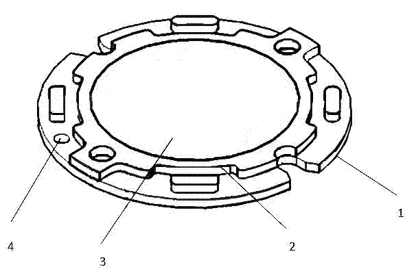
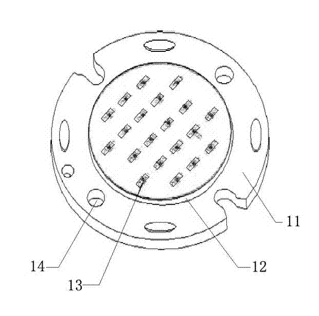
[0033] Reference figure 2 As shown, the novel LED integrated light source module of the present invention includes a substrate body 11, an LED die-bonding area 13, and a colloidal barrier wall 12 formed on the substrate body 1 by mixing and curing white or transparent silica gel and phosphor powder. The retaining wall 12 encloses the die bonding area into at least one enclosed area, the LED chip is arranged in the enclosed area, the height of the colloidal wall is 0.2-10mm, and the distance from the colloidal wall to the LED chip is between 0.05-30mm The colloidal retaining wall of the present invention is preferably a single-component white silicone rubber material; a positioning hole 14 is provided on the main body 11 of the substrate.

[0034] The manufacturing method of the novel LED integrated light source module of the present invention includes th...


PUM


Abstract

The invention discloses a novel LED integrated light source module. The novel LED integrated light source module comprises a substrate body, and LED chips arranged on the substrate body, wherein rubber barrier walls are arranged on the substrate body to enclose an LED chip fixing region on the substrate body to at least one closed region; the LED chips are arranged in the closed region; the rubber barrier walls can stop a phosphor powder glue mixed layer in the LED chip region from flowing out of the light emitting region due to fluid dynamics and can also improve the light emitting efficiency and light uniformity of the LED chip. The invention also discloses a processing method of the above LED integrated light source module.

Description

Technical field [0001] The invention relates to LED packaging technology, in particular to a novel LED integrated light source module and a preparation method thereof. Background technique [0002] As a new type of light source, LED has the characteristics of environmental protection and energy saving, high brightness, long life, fast start-up speed, and high chroma. It is widely used in outdoor advertising displays, indoor lighting, decorative lights and emergency lights. [0003] The method of realizing white light with LED is mainly to use blue LED chip to excite yellow phosphor powder to mix into white light. In the packaging process, the yellow phosphor and glue mixture is mainly used to coat the surface of the chip until the phosphor glue mixed layer reaches a certain level. thickness. Reference figure 1 , In the picture: 1-substrate, 2-compression frame, 3-LED solid crystal spot powder area, 4-positioning hole; in the traditional packaging process, control the thickness of ...

Claims


Application Information

Patent Timeline
Patent Type & Authority Applications(China)
IPC IPC(8): H01L33/54H01L33/00
Inventor 王孟源
Owner FOSHAN EVERCORE OPTOELECTRONICS TECH
Why Eureka
Try Eureka