Chip scale integration packaging process and light emitting diode (LED) device

An LED device and integrated packaging technology, which is applied in the direction of electric solid-state devices, semiconductor devices, electrical components, etc., can solve the problems of reducing the light efficiency of the device, uneven light color, etc., achieve low production costs, reduce light energy loss, and increase luminescence The effect of light color uniformity

Active Publication Date: 2011-06-15
HONGLI ZHIHUI GRP CO LTD
View PDF6 Cites 10 Cited by
  • Summary
  • Abstract
  • Description
  • Claims
  • Application Information

AI Technical Summary

Problems solved by technology

However, using this method of dam control phosphor coating, because the dam itself has a certain absorption effect on the light emitted by the chip, especially the side-emitting chip, especially when the thickness of the dam is too large, the effect of light absorption is very strong. , will greatly reduce the light efficiency of the entire device, and even the problem of uneven light color

Method used


Image

  • Chip scale integration packaging process and light emitting diode (LED) device
  • Chip scale integration packaging process and light emitting diode (LED) device
  • Chip scale integration packaging process and light emitting diode (LED) device

Examples


Embodiment Construction

[0037] The present invention will be further described in detail below with reference to the drawings and specific embodiments.

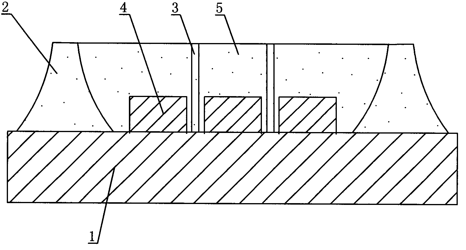
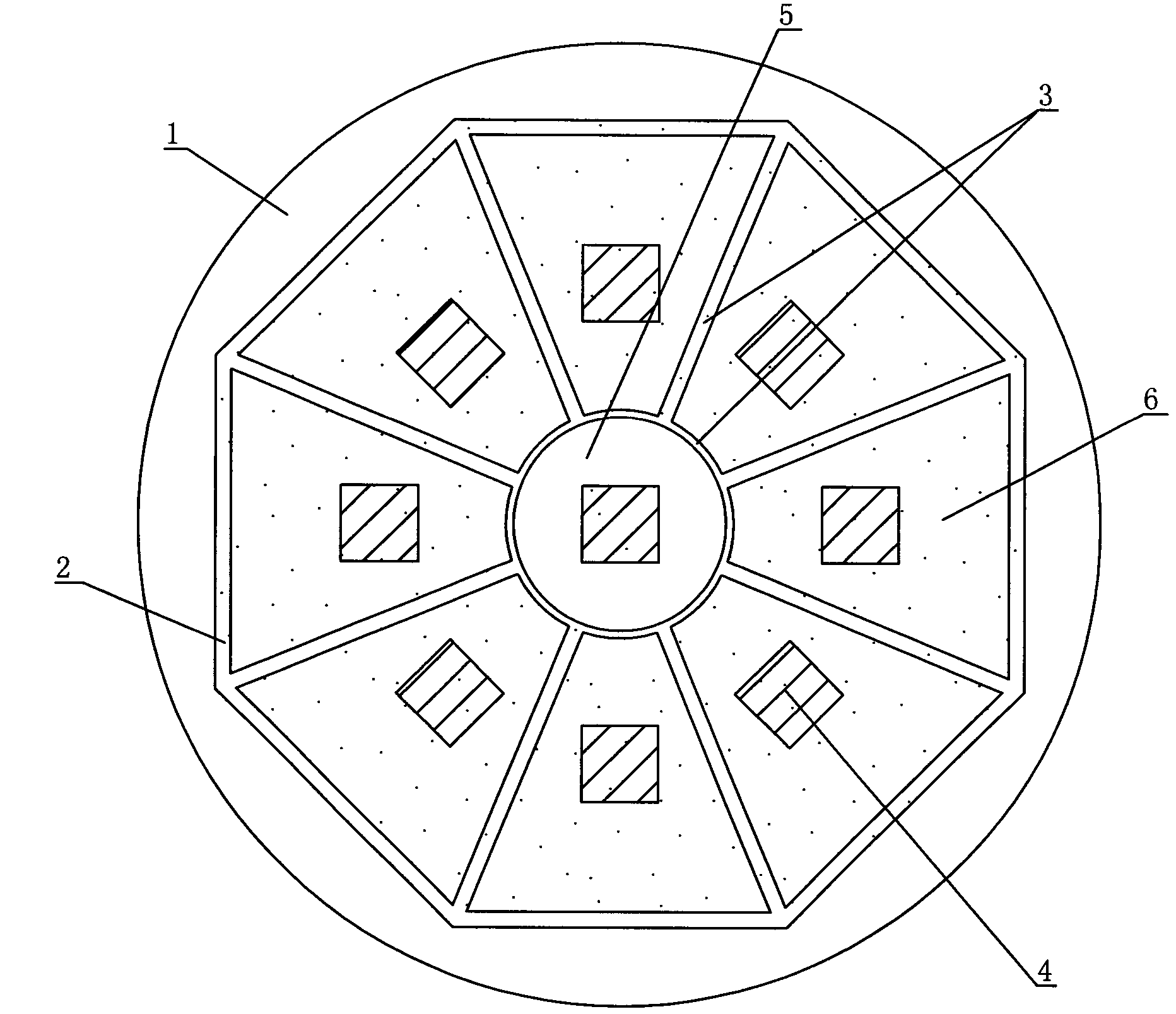
[0038] Such as figure 1 with figure 2 The LED device shown includes a flat panel support 1, which is circular, and the flat panel support 1 is divided into an intermediate area 5 and two or more peripheral areas 6 other than the intermediate area. The intermediate area 5 is Circular, the peripheral area 6 is fan-shaped, and the peripheral area 6 is equally distributed with the center of the intermediate area as the center of the circle. In this embodiment, there are eight peripheral areas 6; LED chips 4 are fixed in the intermediate area 5 and the peripheral area 6, Each area includes more than one LED chip. In this embodiment, one LED chip 4 is installed in each area, wherein the LED chip in the middle area 5 emits red light, and the LED chip in the peripheral area 6 is a blue series; A phosphor glue dam 2 is provided on the flat plate support outsi...


PUM


Abstract

The invention discloses a chip scale integration packaging process and a light emitting diode (LED) device. The packaging process sequentially comprises the following steps of: processing a surface plate substrate, fixing LED chips, coating phosphor glue to form box dam shapes, coating transparent glue to form grating plate shapes, curing the phosphor glue and the transparent glue to form box dams and grating plates, dispensing the phosphor glue in the box dam and drying the phosphor glue. The LED device comprises the surface plate bracket, wherein the surface plate bracket is divided into a central area and more than two peripheral areas outside the central area; the LED chips are fixed in the central and peripheral areas; the phosphor glue box dams are arranged on the surface plate bracket outside the peripheral areas; the grating plates formed by the transparent glue are arranged between the central and peripheral areas and between every two adjacent peripheral areas; and the phosphor glue is packaged in each area. The LED device molded by the packaging process has low optical energy loss, and emits light with uniform light color and high color rendering.

Description

Technical field [0001] The present invention relates to white light LED packaging technology, in particular to white light LED chip-level integrated packaging technology and LED devices applying the technology. Background technique [0002] LED has a series of advantages such as high luminous efficiency, energy saving and environmental protection, long life, small size and stable performance. It has an extremely broad development prospect and is regarded as the most valuable light source in the 21st century. There are many ways to achieve white light for LEDs, among which the most common, most efficient, and lowest-cost method is to use blue or ultraviolet light to excite phosphors and mix them into white light. In the existing packaging process, the main use is to mix phosphors and glue. , Spread on the surface of the chip until the phosphor reaches a certain height of the reflector cup. In the current process, there are mainly two methods to control the shape and amount of pho...

Claims


Application Information

Patent Timeline
Patent Type & Authority Applications(China)
IPC IPC(8): H01L33/00H01L33/48H01L33/50H01L25/13
Inventor 蔡永义谭道礼麦镇强洪琴王跃飞吴乾李国平
Owner HONGLI ZHIHUI GRP CO LTD
Why Eureka
Try Eureka