Optical transmitter and receiver chip structure for synchronously networking by using reverse clock
A technology of clock synchronization and chip structure, which is applied in the direction of synchronous devices, TV systems adapted to optical transmission, cable transmission adaptation, etc., can solve the problems of affecting the integrity of transmitted signals, difficult digital sampling, and difficult data, so as to ensure digital sampling, Simplifies system design and delivers signal-integrated effects
Active Publication Date: 2012-10-17
杭州思泰微电子有限公司
View PDF3 Cites 2 Cited by
- Summary
- Abstract
- Description
- Claims
- Application Information
AI Technical Summary
Problems solved by technology
Bit loss and bit errors occur in the process of digital convergence, which affects the integrity of the transmitted signal
This situation makes it difficult to perform digital sampling when
Method used
View moreImage
Smart ImageViewing Examples

Examples
 PUM
 Abstract
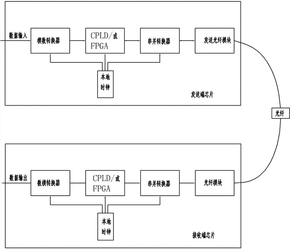
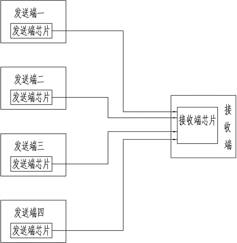
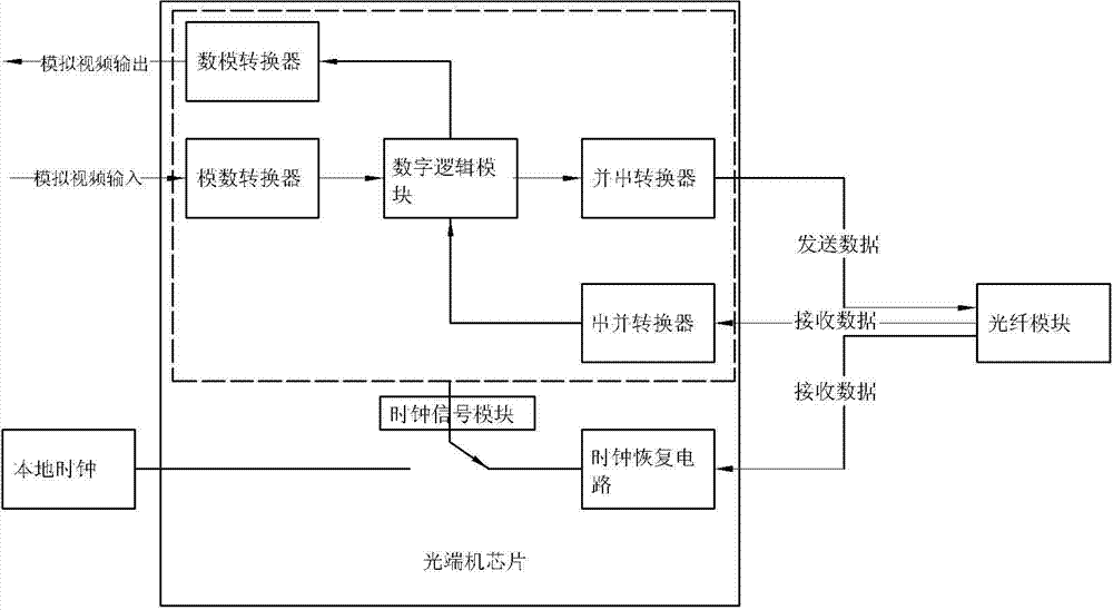
The invention provides an optical transmitter and receiver chip structure for synchronously networking by using a reverse clock. Clock synchronization is carried out among a plurality of chips, therefore, convergence of data among the chips can be realized, and digital sampling of digital convergence is ensured, so that a transmitted signal is enabled to be complete. The optical transmitter and receiver chip structure comprises a digital to analog converter, an analog to digital converter, a digital logic module, a staticizer and a clock signal module, and is characterized by also comprising a clock restoring circuit, a local/remote clock selective switch and a serializer, wherein the output end of the digital to analog converter is externally connected with an analog video output, an analog video input is connected with the input end of the analog to digital converter, the output end of the analog to digital converter is connected with the input end of the digital logic module, the output end of the digital logic module is connected with the input end of the serializer, and the output end of the serializer is externally connected with an optical module through a data line.
Description
technical field [0001] The invention relates to the structural technical field of optical transceivers, in particular to a chip structure of optical transceivers using reverse clock synchronous networking. Background technique [0002] Digital video optical transceivers have been widely used in the field of security monitoring in recent years due to their characteristics of large amount of transmitted data and no transmission loss and delay. [0003] On the other hand, integrated circuit technology has achieved rapid development in recent years with the advancement of technology. Based on deep submicron CMOS technology, the current integrated circuit chip technology can integrate the main functions of video optical transceivers. Digital video optical transceivers based on this integrated chip have greater advantages in terms of power consumption and volume than traditional products. [0004] For the existing digital optical transceiver chip set structure, see figure 1 ...
Claims
Login to View More Application Information
Patent Timeline
 IPC IPC(8): H04N7/22H04L7/00
Inventor 黄海滨吴明远郑可为
Owner 杭州思泰微电子有限公司
Features
- R&D
- Intellectual Property
- Life Sciences
- Materials
- Tech Scout
- Unparalleled Data Quality
- Higher Quality Content
- 60% Fewer Hallucinations
Learn More Browse by: Latest US Patents, China's latest patents, Technical Efficacy Thesaurus, Application Domain, Technology Topic, Popular Technical Reports.
© 2025 PatSnap. All rights reserved.Legal|Privacy policy|Modern Slavery Act Transparency Statement|Sitemap|About US| Contact US: help@patsnap.com