Check patentability & draft patents in minutes with Patsnap Eureka AI!

Electronic device shell and manufacturing method thereof

The technology of an electronic device and manufacturing method is applied in the directions of antenna support/installation device, electrical equipment casing/cabinet/drawer, circuit, etc., and can solve problems such as affecting the service life of electronic devices, easy degumming of antenna, and affecting antenna receiving effect, etc. To achieve the effect of long service life, good signal reception and not easy to separate

Inactive Publication Date: 2012-12-12
SHENZHEN FUTAIHONG PRECISION IND CO LTD
View PDF4 Cites 7 Cited by
  • Summary
  • Abstract
  • Description
  • Claims
  • Application Information

AI Technical Summary

Problems solved by technology

[0004] However, if the electronic device is formed by the above method, the antenna radiator is fixed on the main body by pasting, the antenna is easily degummed and separated from the main body, which affects the service life of the electronic device and the antenna is arranged on the inner wall of the main body, thus affecting The reception effect of the antenna

Method used


Image

  • Electronic device shell and manufacturing method thereof
  • Electronic device shell and manufacturing method thereof

Examples


Embodiment Construction

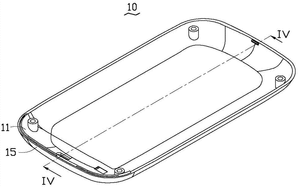
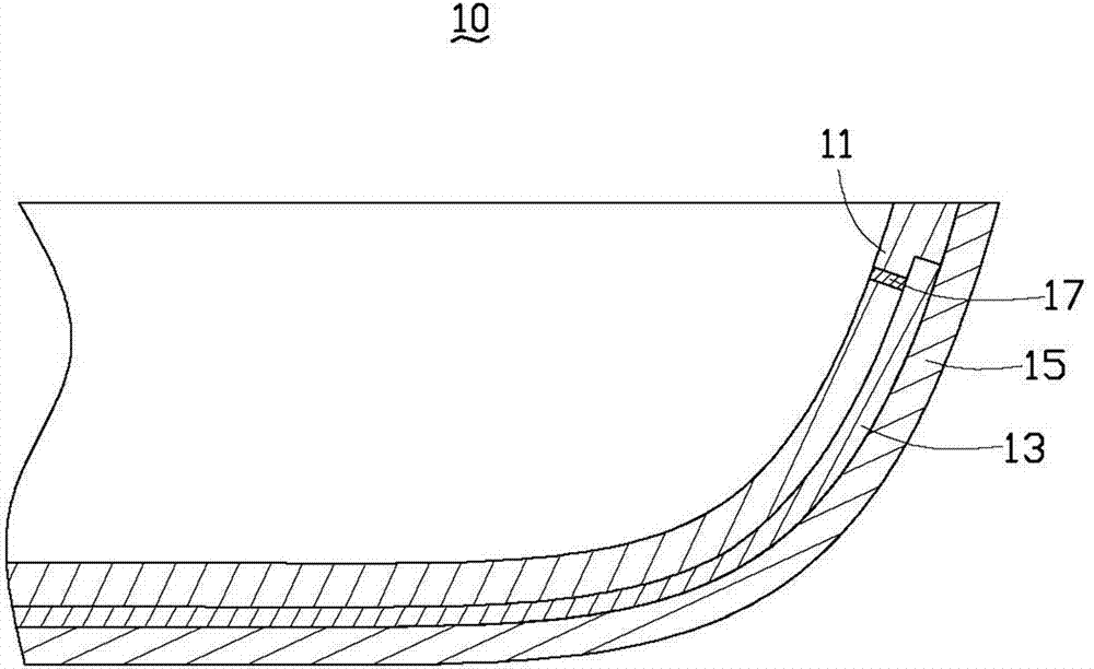
[0018] see figure 1 with figure 2 , The housing 10 of the electronic device according to the preferred embodiment of the present invention includes a base layer 11 , an antenna layer 13 , and a decoration layer 15 . The base layer 11 is formed by injecting plastic through injection molding, the antenna layer 13 is formed on the outer surface of the base layer 11 by injecting conductive plastic, and the decoration layer 15 is formed on the antenna layer by magnetron sputtering or non-conductive vacuum plating 13, and completely cover the antenna layer 13, of course, the decorative layer 15 can also partially cover the antenna layer 13.

[0019] The electronic device casing 10 further includes a conductive element 17 , the conductive element 17 is embedded on the base layer 11 and electrically connected to the antenna layer 13 .

[0020] The base layer 11 of the electronic device casing 10 is made by injection molding, and the conductive element 17 is embedded therein. Plast...


PUM

PropertyMeasurementUnit
sizeaaaaaaaaaa
diameteraaaaaaaaaa
lengthaaaaaaaaaa

Abstract

The invention provides an electronic device shell and a manufacturing method of the electronic device shell. The electronic device shell comprises a base body layer, an antenna layer and a decorative layer, wherein the antenna layer is molded on the outer surface of the base body layer through injection moulding of conductive plastics, the antenna layer is covered by the decorative layer, an antenna layer of the electronic device shell is covered by a formation layer, and an antenna and a base body are hard to separate. The electronic device shell has the advantages of long service life and favorable signal receiving effect.

Description

technical field [0001] The invention relates to an electronic device casing, in particular to an electronic device casing with an antenna on the outer layer of the casing and a manufacturing method thereof. Background technique [0002] With the development of technologies such as mobile communication and bluetooth, electronic devices for these applications have more and more functions. However, the volume of these electronic devices is becoming lighter and thinner. Therefore, how to simplify the built-in components of these electronic devices The structure of the structure and the reduction of the volume of these built-in components play a very important role in simplifying the structure of the entire electronic device and reducing the volume of the electronic device. An antenna is an important component for sending and receiving signals in an electronic device, and its structure simplification and volume reduction play an important role in simplifying the structure of the ...

Claims


Application Information

Patent Timeline
Patent Type & Authority Applications(China)
IPC IPC(8): H05K5/00H01Q1/22H01Q1/38C23C14/06C23C14/34
CPCC23C14/0652H01Q1/40H01Q1/243
Inventor 吴照毅阎勇樊永发张薛丽
Owner SHENZHEN FUTAIHONG PRECISION IND CO LTD
Features
  • R&D
  • Intellectual Property
  • Life Sciences
  • Materials
  • Tech Scout
  • Unparalleled Data Quality
  • Higher Quality Content
  • 60% Fewer Hallucinations
Learn More