Forming method of stress semiconductor groove

A semiconductor and channel technology, applied in the formation of strained semiconductor channels, can solve the problems of difficult to control etching depth, loss of strained Si coating, relaxation of strained Si coating, etc., to avoid loss of semiconductor layer and reduce processing Steps, Effects of Controlling Etching Depth

Active Publication Date: 2015-04-08
INST OF MICROELECTRONICS CHINESE ACAD OF SCI
View PDF4 Cites 0 Cited by
  • Summary
  • Abstract
  • Description
  • Claims
  • Application Information

AI Technical Summary

Problems solved by technology

However, in conventional strained Si channel formation methods, prior to device fabrication processes (e.g., shallow trench isolation (STI), gate formation, etc.), a strained Si cladding layer must first be formed on, for example, a SiGe layer.
This also leads to the following problems: (1) The strained Si cap may be depleted during the device fabrication process, for example, pad oxidation in STI process, sacrificial oxidation before gate formation process, various wet chemical Depletion of the strained Si cladding may occur due to cleaning treatments, etc.; (2) The strained Si cladding may relax (stress is released) during high temperature steps, e.g. annealing for activating source / drain dopants Processing may cause the stress in the strained Si cladding to be released
However, in this solution, the SiGe single material is etched, and there is a problem that the etching depth is difficult to control due to the selectivity ratio.
Although SiGe can be used to form an etching stop layer, it will undoubtedly increase the process difficulty of epitaxial growth, and the effect of controlling etching is not obvious

Method used


Image

  • Forming method of stress semiconductor groove
  • Forming method of stress semiconductor groove
  • Forming method of stress semiconductor groove

Examples


Embodiment Construction

[0026] One or more aspects of embodiments of the invention are described below with reference to the drawings, wherein like reference numerals generally refer to like elements throughout. In the following description, for purposes of explanation, numerous specific details are set forth in order to provide a thorough understanding of one or more aspects of the embodiments of the invention. It may be apparent, however, to one skilled in the art that one or more aspects of the embodiments of the invention may be practiced with a lesser degree of these specific details.

[0027] In addition, although a particular feature or aspect of an embodiment is disclosed in terms of only one of some implementations, such feature or aspect may be combined with other implementations that may be desirable and advantageous for any given or particular application. One or more other features or aspects of .

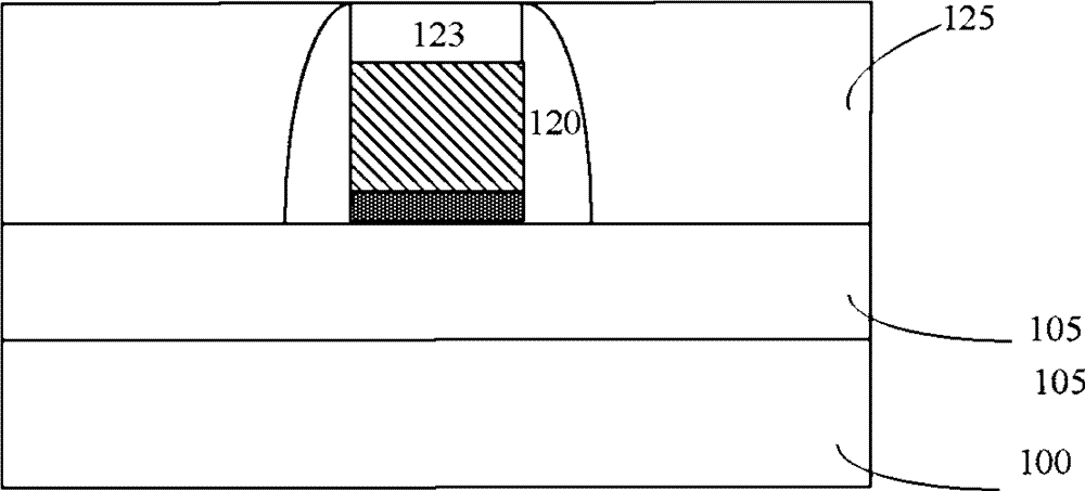
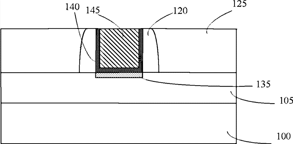
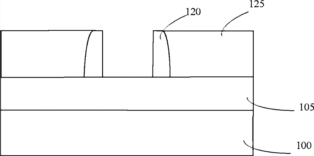
[0028] First, a relaxed layer 105 is formed on a substrate 100 (such as Si, silicon-on-i...


PUM


Abstract

A method for forming a strained semiconductor channel. A strained channel is formed after annealing of the source / drain, so that the strained semiconductor channel is prevented from being exposed to the high temperature source / drain annealing treatment. Furthermore, the treatment steps that the strained semiconductor channel is to undergo are reduced, thereby avoiding the loss of the semiconductor layer. In addition, the etching rate at the ion implantation region is obviously greater than the etching rate at the relaxed layer part without ion implantation, so that the etching depth can be easily controlled.

Description

technical field [0001] The invention relates to the field of semiconductors, in particular to a method for forming a strained semiconductor channel. Background technique [0002] With the continuous reduction of device feature size, strained channel engineering for the purpose of improving channel carrier mobility plays an increasingly important role. Theoretical and empirical studies have demonstrated that when stress is applied to the channel of a transistor, the carrier mobility of the transistor is enhanced or decreased; however, it is also known that electrons and holes respond differently to the same type of strain . For example, applying compressive stress in the direction of current flow is beneficial to hole mobility but detrimental to electron mobility. The tensile stress is beneficial to the electron mobility, but harmful to the hole mobility. Specifically, for NMOS devices, the introduction of tensile stress along the channel direction increases the mobility o...

Claims


Application Information

Patent Timeline
Patent Type & Authority Patents(China)
IPC IPC(8): H01L21/336H01L21/8238
CPCH01L29/66545H01L21/26513H01L29/1054H01L29/78H01L21/3065H01L29/165
Inventor 尹海洲骆志炯朱慧珑
Owner INST OF MICROELECTRONICS CHINESE ACAD OF SCI
Why Eureka
Try Eureka