Integrally molded die and bezel structure for fingerprint sensors and the like

A fingerprint sensor and sensor array technology, which can be used in the acquisition/organization of fingerprints/palmprints, instruments, electrical solid-state devices, etc., and can solve problems such as constraints

Inactive Publication Date: 2012-12-26
APPLE INC
View PDF8 Cites 17 Cited by
  • Summary
  • Abstract
  • Description
  • Claims
  • Application Information

AI Technical Summary

Problems solved by technology

However, the known separate inlay and encapsulated die designs limit the possible options for final device size and sensor-inlay spacing

Method used


Image

  • Integrally molded die and bezel structure for fingerprint sensors and the like
  • Integrally molded die and bezel structure for fingerprint sensors and the like
  • Integrally molded die and bezel structure for fingerprint sensors and the like

Examples


Embodiment Construction

[0025] At the outset, it is pointed out that descriptions of well-known materials, processing techniques, components, equipment, and other well-known details are either schematically outlined or are omitted so as not to unnecessarily obscure the invention in detail. Thus, where some details are otherwise known, it will be up to the application of the invention to suggest or dictate choices relating to these details.

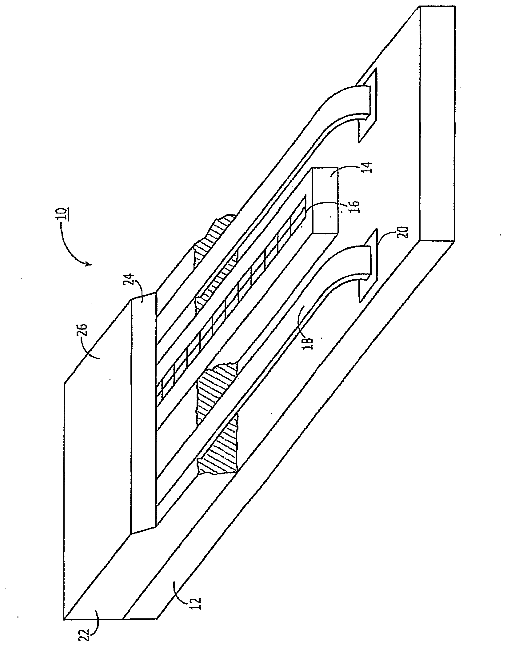
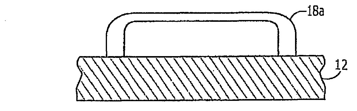
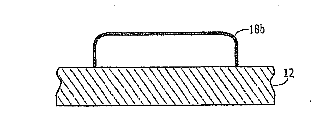
[0026] first reference figure 1 , which shows a partially cutaway perspective view of the biometric sensor assembly 10 according to the first embodiment. Assembly 10 includes a substrate 12 , which may be a printed circuit board (PCB), ceramic body, or similar structure, having interconnect leads (not shown) formed thereon and possibly in various layers thereof. A sensor integrated circuit or die 14 is secured to a die receiving area of ​​substrate 12 . Die 14 is typically a semiconductor body having formed thereon one or more layers including electrical device...


PUM


Abstract

A biometric sensor device, such as a fingerprint sensor, comprises a substrate to which is mounted a die on which is formed a sensor array and at least one conductive bezel. The die and the bezel are encased in a unitary encapsulation structure to protect those elements from mechanical, electrical, and environmental damage, yet with a portion of the sensor array and the bezel exposed or at most thinly covered by the encapsulation or other coating material structure.

Description

technical field [0001] The present disclosure relates to integrated circuit packaging, and more particularly, to methods and apparatus for integrally molding a die and one or more slug structures for fingerprint sensors and the like, wherein the die and slug structures Parts of each are exposed or at best thinly covered. Background technique [0002] One of the more common biometric sensing devices today is the fingerprint sensor. These devices control access to electronic devices such as computers and mobile phones, safes, buildings, vehicles, etc. by scanning a user's fingerprint and comparing it to a set of authenticated fingerprint images. Access may be granted if the provided fingerprint to be authenticated (as-taken) matches one of a set of pre-registered authorized fingerprints. The fingerprint sensor may be a standalone device, integrated into other devices such as PC peripherals, or may be integrated into the device through which the sensor controls access. The s...

Claims


Application Information

Patent Timeline
Patent Type & Authority Applications(China)
IPC IPC(8): G06K9/00
CPCG06K9/00053H01L27/20G06K9/0002H01L2224/48091G06V40/1306H01L2924/00014G06V10/10G06V40/1329H10N39/00
Inventor R·H·邦德A·拉卡梅尔G·戈齐尼
Owner APPLE INC
Why Eureka
Try Eureka