Scanning drive circuit of liquid crystal panel, liquid crystal display device and driving method

A technology for scanning driving circuits and liquid crystal display devices, applied in static indicators, instruments, etc., can solve the problem of occupying the edge of the glass, and achieve the effect of reducing the difficulty of binding, reducing the number, and reducing the cost of packaging

Active Publication Date: 2013-01-23
TCL CHINA STAR OPTOELECTRONICS TECH CO LTD
View PDF9 Cites 20 Cited by
  • Summary
  • Abstract
  • Description
  • Claims
  • Application Information

AI Technical Summary

Problems solved by technology

[0004] At present, the mainstream design of LCD panels is developing towards narrow bezels, and they are trying to reduce the design of the glass edge in various ways as much as possible. Every small space saving may be crucial, so too many wires will occupy the The space at the edge of the glass, it is necessary to reduce the number of traces

Method used


Image

  • Scanning drive circuit of liquid crystal panel, liquid crystal display device and driving method
  • Scanning drive circuit of liquid crystal panel, liquid crystal display device and driving method
  • Scanning drive circuit of liquid crystal panel, liquid crystal display device and driving method

Examples


Embodiment Construction

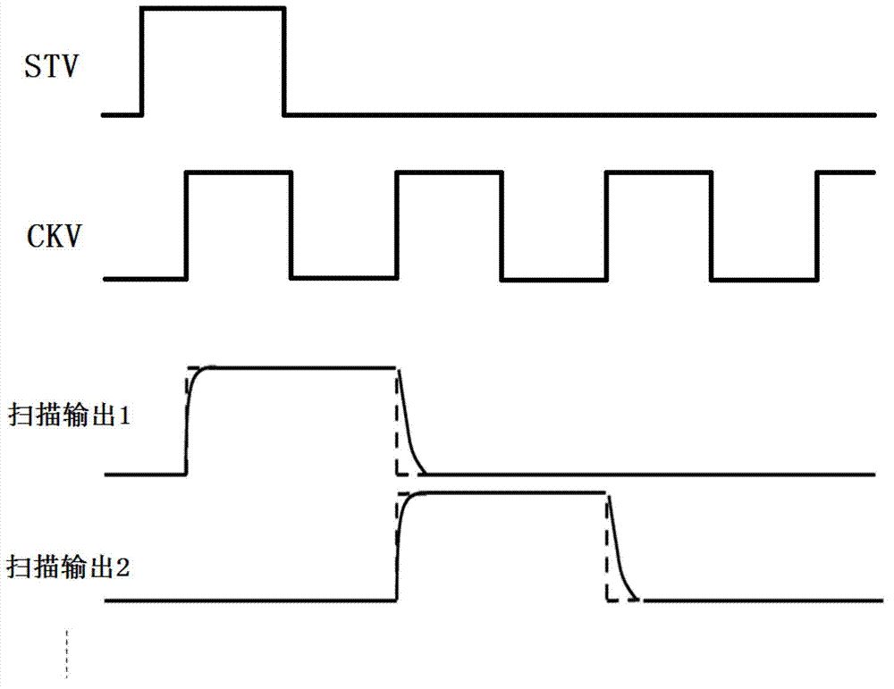
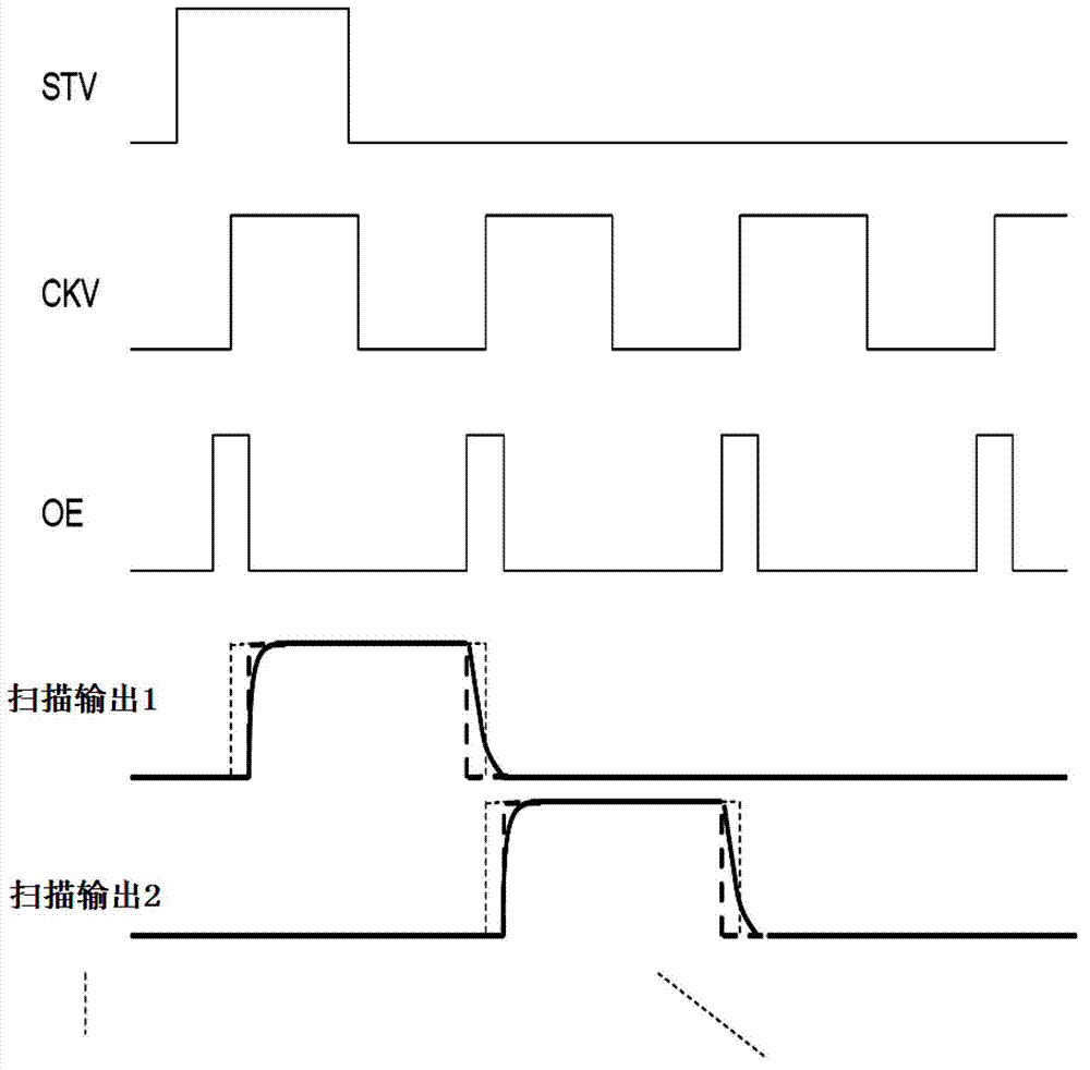
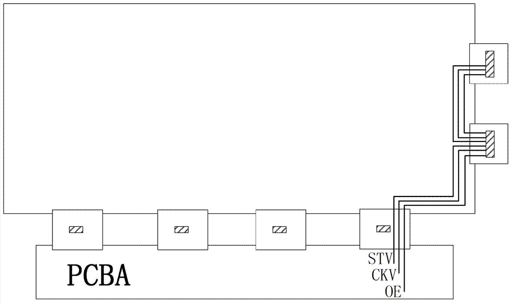
[0026] A scanning driving circuit of a liquid crystal panel, the driving circuit of the liquid crystal panel includes a delay component, an input end of the delay component is coupled to an enable control signal, an output end is coupled to a clock pulse signal, and the delay component is The delay time is less than the action time of a single enable control signal.

[0027] Since the present invention adopts the delay component, the delay component can delay the output of the same input signal, and the pulse width of each scan line drive is related to the signal width of one cycle of the clock pulse signal, which is related to the clock pulse signal in one cycle. The pulse width of the high-level signal is not directly related. Therefore, keep the pulse width of the clock pulse signal consistent with the pulse width of the enable control signal, so that signal multiplexing can be achieved through the delay component, and the input end of the delay component It is an enabling ...


PUM


Abstract

The invention discloses a scanning drive circuit of a liquid crystal panel, a liquid crystal display device and a driving method. The drive circuit of the liquid crystal panel comprises a time delay component, wherein the input end of the time delay component is coupled to an enable control signal while the output end of the time delay component is coupled to a clock pulse signal, and the delayed time of the time delay component is less than the action time of single enable control signal. According to the drive circuit provided by the invention, the amount of control signal lines of a scanning chip is reduced, and a space for narrow bezel design is obtained; in addition, the control lines pass through a COF (Chip On Film), the amount of the control lines is reduced, the spacing between the control lines is increased, and the binding difficulty of the COF is reduced; and moreover, the amount of pins of the corresponding chip also can be reduced, and the packaging cost of the chip is reduced.

Description

technical field [0001] The present invention relates to the field of liquid crystal display, and more particularly, to a scanning driving circuit of a liquid crystal panel, a liquid crystal display device and a driving method. Background technique [0002] The liquid crystal display panel includes criss-cross scan lines and control lines, and the scan lines are controlled by scan driving chips arranged on both sides of the liquid crystal panel. At present, there are three control signals required by the scan driver chip to control the opening and closing of each line of the liquid crystal display. They are the start pulse signal STV (start voltage pulse), which controls the start of the first line; the clock pulse signal CKV (clock voltage pulse), which It is provided to the shift register of the scan driver chip to control the switching frequency of each row, and starts to act when the rising edge detects that STV is at a high level; the output enable control signal OE (out...

Claims


Application Information

Patent Timeline
Patent Type & Authority Applications(China)
IPC IPC(8): G09G3/36
CPCG09G3/3677
Inventor 郭东胜
Owner TCL CHINA STAR OPTOELECTRONICS TECH CO LTD
Why Eureka
Try Eureka