Silicon wafer carrying device

A technology for carrying devices and silicon wafers, applied in transportation, packaging, conveyors, etc., can solve the problems of increasing the production cost of silicon wafer manufacturers, and achieve the effects of avoiding bumps or shocks, reducing damage, and reducing production costs

Inactive Publication Date: 2013-01-30
ZHEJIANG YUHUI SOLAR ENERGY SOURCE
View PDF5 Cites 3 Cited by
  • Summary
  • Abstract
  • Description
  • Claims
  • Application Information

AI Technical Summary

Problems solved by technology

The damaged silicon wafer needs to be returned to the initial manufacturing process for remanufacturing, which increases the production cost of the silicon wafer manufacturer

Method used


Image

  • Silicon wafer carrying device
  • Silicon wafer carrying device
  • Silicon wafer carrying device

Examples


Embodiment Construction

[0028] The invention provides a silicon chip carrying device, which reduces the damage of the silicon chip in the transportation process, and further reduces the production cost of the silicon chip manufacturer.

[0029] The following will clearly and completely describe the technical solutions in the embodiments of the present invention with reference to the accompanying drawings in the embodiments of the present invention. Obviously, the described embodiments are only some, not all, embodiments of the present invention. Based on the embodiments of the present invention, all other embodiments obtained by persons of ordinary skill in the art without making creative efforts belong to the protection scope of the present invention.

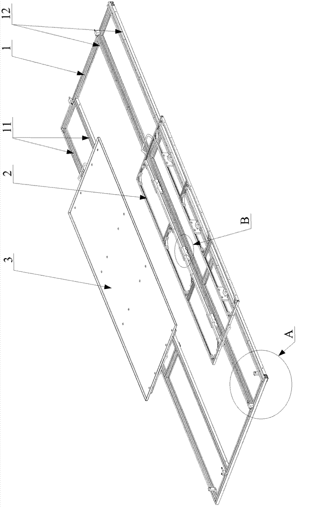
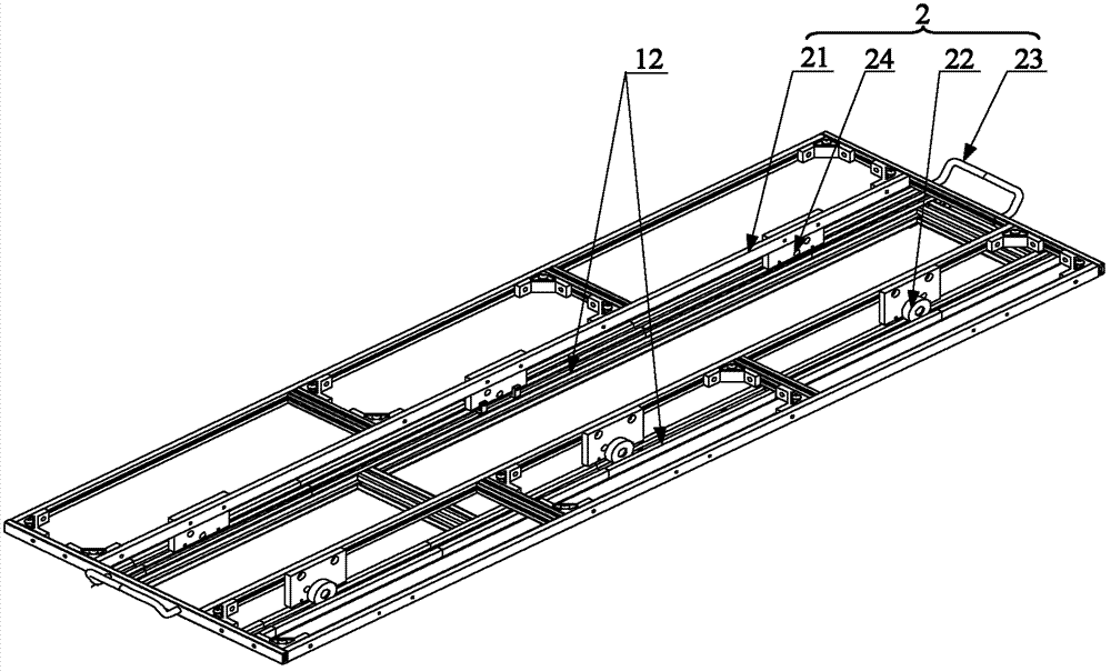
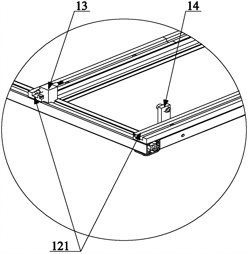
[0030] Please refer to the attached Figure 1-4 , figure 1 Schematic diagram of the structure of the silicon wafer carrying device provided by the embodiment of the present invention; figure 2 It is a schematic diagram of the cooperation structure...


PUM


Abstract

The invention provides a silicon wafer carrying device which comprises a support frame (1) and a carrying trolley. The support frame (1) is provided with tracks, roller grooves (121) are arranged on the tracks (12), and the carrying trolley is positioned on the support frame (1) and is provided with silica-gel rollers (22) which are matched with the roller grooves (121) in a rolling manner. The silicon wafer carrying device has the advantages that damage to silicon wafers in a transportation process is reduced, and accordingly production cost is lowered for a silicon wafer manufacturer.

Description

technical field [0001] The invention relates to the technical field of silicon wafer production auxiliary equipment, and more specifically relates to a silicon wafer carrying device. Background technique [0002] The solar photovoltaic industry is one of the fastest growing energy industries in the world. With the support of the governments of various countries, the solar photovoltaic power generation industry has developed rapidly since the 1980s. Silicon material is an essential material for photovoltaic equipment, so the rapid development of the solar photovoltaic industry has brought good development opportunities for upstream silicon wafer production. By 2010, the annual demand for solar silicon wafers had reached 280,520 pieces. With the increasing use of silicon wafers, reducing the damage of silicon wafers in the production process to reduce production costs is the top priority of silicon wafer manufacturers. [0003] During the production process of silicon wafer...

Claims


Application Information

Patent Timeline
Patent Type & Authority Applications(China)
IPC IPC(8): B65G21/22
Inventor 刘琴
Owner ZHEJIANG YUHUI SOLAR ENERGY SOURCE
Why Eureka
Try Eureka