Wafer level packaging method for image sensor

A wafer-level packaging and image sensor technology, applied in the semiconductor field, can solve the problems of low process yield and increased production cost of image sensors.

Active Publication Date: 2013-01-30
GALAXYCORE SHANGHAI
View PDF4 Cites 16 Cited by
  • Summary
  • Abstract
  • Description
  • Claims
  • Application Information

AI Technical Summary

Problems solved by technology

[0005] In addition, the process yield of the image sensor with the add

Method used


Image

  • Wafer level packaging method for image sensor
  • Wafer level packaging method for image sensor
  • Wafer level packaging method for image sensor

Examples


Embodiment Construction

[0025] The making and using of the embodiments are discussed in detail below. It should be understood, however, that the specific embodiments discussed are merely illustrative of specific ways to make and use the invention, and do not limit the scope of the invention.

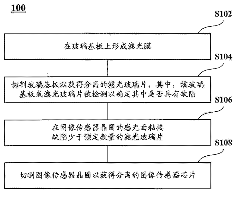
[0026] figure 2 A flow of a wafer-level packaging method 100 for an image sensor according to an embodiment of the present invention is shown.

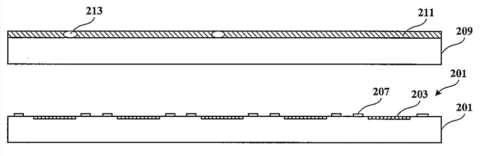
[0027] Such as figure 2 As shown, the packaging method 100 includes: performing step S102, forming a filter film on a glass substrate; performing step S104, cutting the glass substrate to obtain a separate filter glass, wherein the glass substrate or filter glass is detected To determine whether there is a defect; Execute step S106, bond the filter glass with defects less than a predetermined number on the photosensitive surface of the image sensor wafer; Execute step S108, cut the image sensor wafer to obtain separated image sensor chips.

[0028] It can be seen ...


PUM


Abstract

The invention provides a wafer level packaging method for an image sensor. The packaging method comprises the following steps of: (a) forming a film filter on a glass substrate; (b) cutting the glass substrate so as to obtain separated filtering glass pieces, and detecting the glass substrate or the filtering glass pieces so as to judge whether defects exist in the glass substrate or the filtering glass pieces; (c) and adhering filtering glass pieces with defects smaller than the preset quantity to a light sensing surface of a wafer of the image sensor; and (d) cutting the wafer of the image sensor so as to obtain separated chips of the image sensor.

Description

technical field [0001] The present invention relates to the technical field of semiconductors, and more particularly, to a wafer-level packaging method for an image sensor. Background technique [0002] An image sensor is a sensor that senses external light and converts it into an electrical signal. Image sensors are typically chip-fabricated using semiconductor manufacturing processes. After the image sensor chip is manufactured, a series of packaging processes are performed on the image sensor chip to form a packaged image sensor for use in various electronic devices such as digital cameras and digital video cameras. [0003] figure 1 A package structure of an image sensor is shown. Such as figure 1 As shown, the package structure includes: an image sensor chip 11 , a package glass 12 , a filter glass 13 , an optical lens 14 and a bracket 15 . Wherein, the packaging glass 12 is supported on the side of the photosensitive surface of the image sensor chip 11 by the supp...

Claims


Application Information

Patent Timeline
IPC IPC(8): H01L27/146
Inventor 李文强
Owner GALAXYCORE SHANGHAI
Why Eureka
Try Eureka