
Pixel structure of transparent liquid crystal display panel

一种透明液晶显示、像素结构的技术,应用在非线性光学、仪器、光学等方向,能够解决显示画面色饱和度降低、背景影像模糊、穿透光绕射等问题

Inactive Publication Date: 2013-05-08
AU OPTRONICS CORP
View PDF9 Cites 22 Cited by
  • Summary
  • Abstract
  • Description
  • Claims
  • Application Information

AI Technical Summary

Problems solved by technology

However, when the multi-area vertically aligned liquid crystal display panel is applied to a transparent liquid crystal display panel that can switch between the transparent display mode and the image display mode, the arrangement of liquid crystal molecules in multiple alignment areas is likely to cause diffraction of transmitted light, so in the transparent display mode Can produce blurred background images
In addition, in the picture display mode, the color saturation of the display picture will also be affected by the penetrating light of the background and reduce

Method used


Image

  • Pixel structure of transparent liquid crystal display panel
  • Pixel structure of transparent liquid crystal display panel
  • Pixel structure of transparent liquid crystal display panel

Examples


Embodiment Construction

[0087] In order to enable those who are familiar with the technical field of the present invention to further understand the present invention, the preferred embodiments of the present invention are listed below, together with the attached drawings, to describe in detail the composition of the present invention and the desired effects .

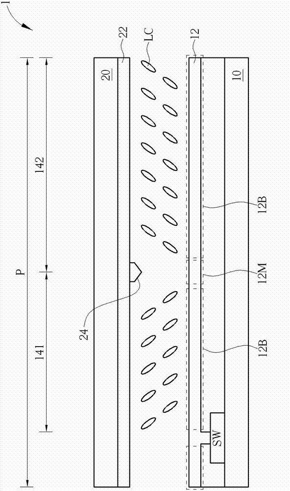
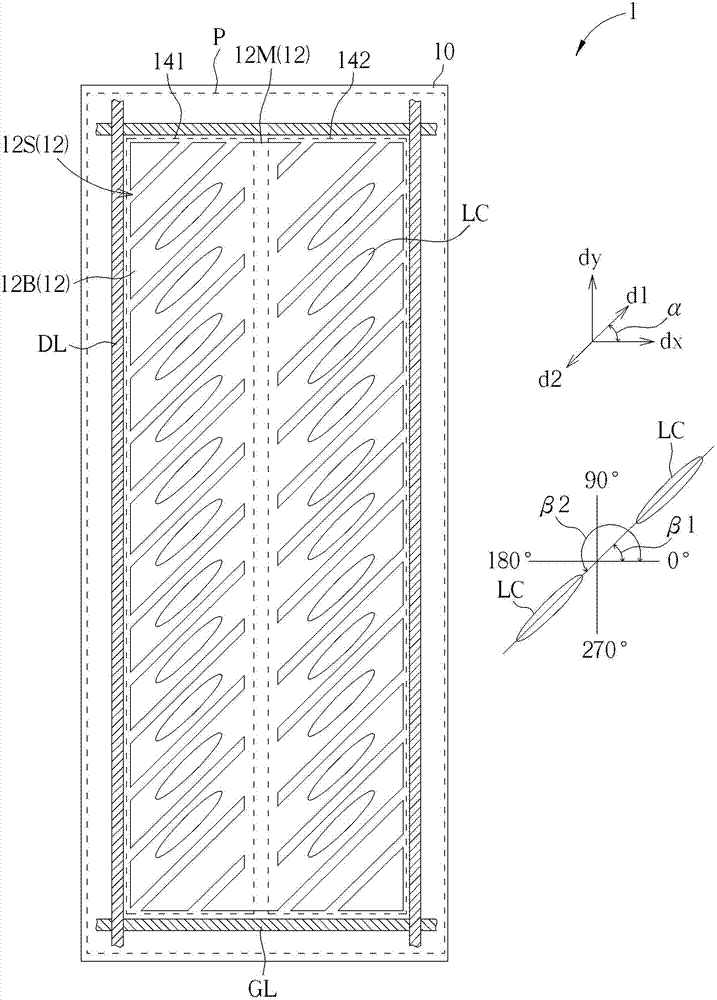
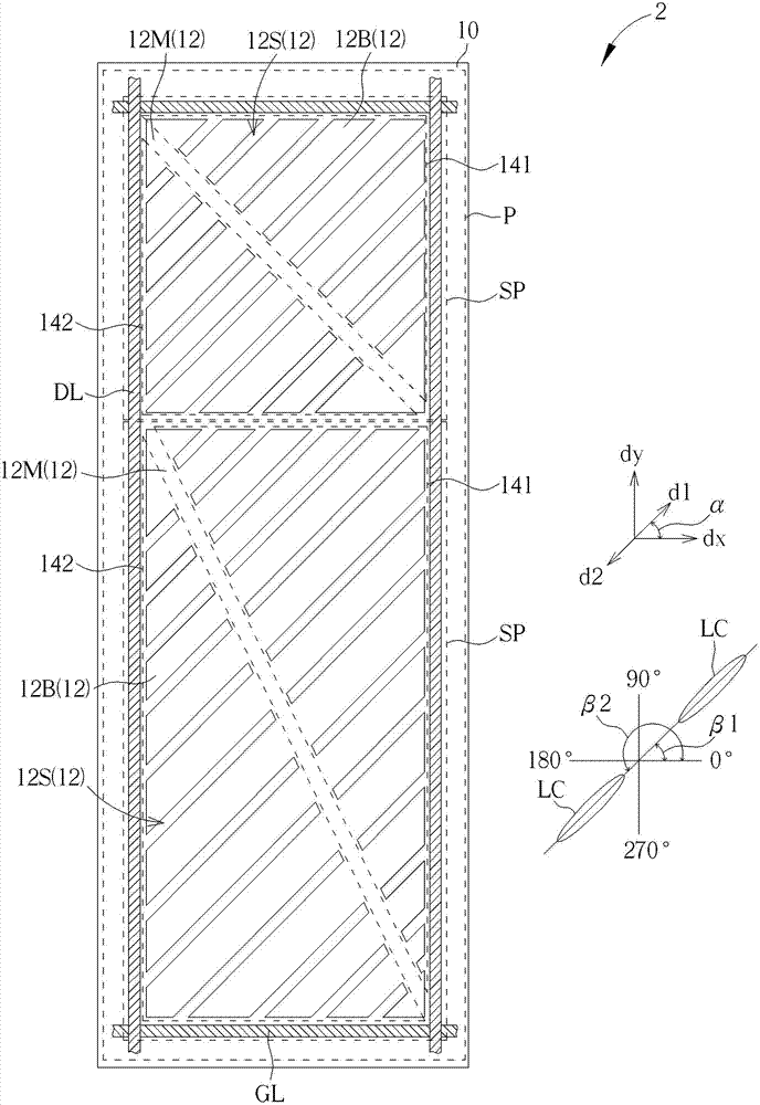
[0088] Please refer to figure 1 and figure 2 . figure 1 A schematic cross-sectional view illustrating a pixel structure of a transparent liquid crystal display panel according to a first embodiment of the present invention, figure 2 painted figure 1 A schematic top view of the array substrate of the pixel structure of the transparent liquid crystal display panel. Such as figure 1 and figure 2 As shown, the pixel structure 1 of the transparent liquid crystal display panel of this embodiment includes an array substrate 10, a gate line GL, a data line DL, an active switching element SW, a pixel electrode 12, a pixel P, an opposite subst...


PUM


Abstract

The present invention relates to a pixel structure of a transparent liquid crystal display panel, which comprises the following components: a pixel, a pixel electrode and liquid crystal modules. The pixel is composed of a first aligning area and a second aligning area with different aligning directions. The pixel electrode comprises a main electrode and a plurality of branch electrodes. The main electrode is a linear main electrode. Partial branch electrodes are connected with one side of the main electrode and outwards extend to a first aligning area along a first direction, and the other branch electrodes are connected with the other side of the main electrode and outwards extend to a second aligning area along a second direction. Furthermore a slit is provided between two random branch electrodes. The first direction is approximately opposite with and parallel with the second direction. Furthermore an included angle between the first direction and a grid line is 45+ / -10 DEG. The pixel structure provided by the invention can settle a problem of low resolution of the background image.

Description

technical field [0001] The present invention relates to a pixel structure of a transparent liquid crystal display panel, in particular to a pixel structure of a transparent liquid crystal display panel capable of avoiding background image blur and having high transmittance. Background technique [0002] The liquid crystal display panel has the advantage of being thin, light and small, and has been widely used in various electronic products, such as smart phones (smart phones), personal digital assistants (PDAs), and notebook computers (notebooks). However, since the liquid crystal display panel usually has the disadvantage of narrow viewing angle, which has become a restrictive condition for development, the industry has developed a multi-domain vertical alignment (MVA) liquid crystal display panel because of its wide viewing angle. characteristics, thus becoming the mainstream product of large-size flat-panel display panels. [0003] The pixel structure of the multi-region...

Claims


Application Information

Patent Timeline
Patent Type & Authority Applications(China)
IPC IPC(8): G02F1/1362G02F1/1343G02F1/1337
CPCG02F1/133514G02F1/1362G02F2201/52G02F1/134309G02F1/133707G02F1/1412G02F1/133742G02F1/134345G02F1/1368
Inventor 郭家玮廖宜扬林敬桓郭庭玮辛坤莹曾柏翔刘康弘吕仁贵杉浦规生
Owner AU OPTRONICS CORP
Learn More