Substrate film for transparent electrode film production

A technology of transparent electrode film and transparent electrode layer, which is applied in the direction of cable/conductor manufacturing, circuits, electrical components, etc., and can solve problems such as mechanical damage, inability to develop electrode layers, and cracking of ITO layers

Inactive Publication Date: 2014-07-30
INSCON TECH +2
View PDF0 Cites 3 Cited by
  • Summary
  • Abstract
  • Description
  • Claims
  • Application Information

AI Technical Summary

Problems solved by technology

[0004] However, for the ITO film, due to the formation of a thinner strong mechanically brittle metal oxide on the surface of the flexible polymer substrate material, the surface ITO layer may be ruptured during thermal shock, and thus cannot function as an electrode layer.
In particular, when high heat and high humidity are applied in the aging test, that is, at a temperature equal to or higher than the glass transition temperature of the substrate film (for example, when the substrate film is PET, the aging test is carried out by subjecting the substrate film to 85 ℃ and 85% relative humidity for 120 hours; 85 ℃ / 85% RH / 120 hours test) when the test is carried out when high humidity is applied, the surface metal oxide layer may be due to the substrate film and Mechanical damage occurs due to thermal expansion or thermal contraction differences between ITO layers, resulting in undesirable cracks
In addition, since the electrode layer is formed of a highly brittle metal oxide, when a force is applied thereon to input letters, the surface metal oxide layer may also be mechanically broken, thereby causing the undesirable problem that the input can no longer be recognized. the letters of

Method used


Image

  • Substrate film for transparent electrode film production

Examples


Embodiment 1

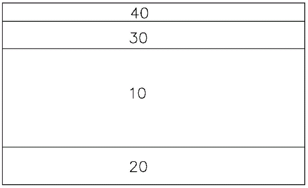
[0055] A semi-cured layer whose curing degree was adjusted to 60% by controlling the light dose was formed on one surface of a 188 μm thick polyester film.

[0056] In this way, the photocurable resin composition used is mixed with 10g of trifunctional acrylate monomer, 10g of trifunctional aliphatic acrylate oligomer, 10g of hexafunctional acrylate oligomer, 2g of 265nm initiator and 68g of acetic acid. Made from ethyl ester. The photocurable composition is dried to a coating thickness of 5μm, and the UV dose applied when forming a cured layer is 600mJ / cm 2 .

[0057] The subsequent process was performed in a similar manner to Comparative Example 1, except that the PEDOT composition of Comparative Example 1 was applied on the surface of the semi-cured layer and then dried to form an electrode layer.

[0058] The X-axis terminal resistance of the manufactured touch unit is 276Ω, and the Y-axis terminal resistance is 575Ω.

[0059] The adhesive force of the electrode layer of the touc...

Embodiment 2

[0061] A fully cured photocurable layer is formed on one surface of a 188μm thick polyester film, and the same resin is applied on the other surface, thereby forming a semi-cured layer with a curing degree of 60% by adjusting the light dose .

[0062] The photocurable resin composition used was mixed with 10g of trifunctional acrylate monomer, 10g of trifunctional aliphatic acrylate oligomer, 10g of hexafunctional urethane acrylate oligomer, 2g of 265nm initiator and 68g Made with ethyl acetate. The photocurable composition is dried to a coating thickness of 5μm, and the UV dose applied when forming a fully cured layer is 600mJ / cm 2 .

[0063] The subsequent process was performed in a similar manner to Comparative Example 1, except that the PEDOT composition of Comparative Example 1 was applied on the surface of the semi-cured layer and then dried to form an electrode layer, and a fully cured layer was formed.

[0064] The X-axis terminal resistance of the manufactured touch unit i...

Embodiment 3

[0067] Example 3 is similar to Example 2, except that the degree of curing of the semi-cured layer is 75%.

[0068] The X-axis terminal resistance of the manufactured touch unit is 265Ω, and the Y-axis terminal resistance is 587Ω.

[0069] The adhesion force of the electrode layer of the touch module manufactured according to ASTM D3359 is 5B (which is evaluated as good), and the change of the terminal resistance after the aging test is measured: the upper template is 6.7%, and the lower template is -6.5%. The haziness of this sample is 1.96%.


PUM

PropertyMeasurementUnit
thicknessaaaaaaaaaa
electrical resistanceaaaaaaaaaa

Abstract

The present invention relates to a technique for producing a transparent electrode film by forming transparent electrode raw materials such as a conductive polymer, carbon nanotubes, graphene and metallic nanowire on the surface of a transparent substrate of polyester or the like, wherein, in order to reduce changes in the surface resistance of the transparent electrode film during edge testing, a photocurable resin layer is formed on the surfaces on both sides of the substrate film, and a transparent electrode layer is formed on the surface on one face thereof. Here, the technique involves adjusting the degree of photocuring of the photocurable layers formed on the surfaces on both sides of the substrate film such that the degree of curing of a face on one side is at least 85%, and the degree of curing of the photocurable resin layer on the opposite surface is between 45 and 85% and then forming the transparent electrode layer on this surface.

Description

Technical field [0001] The present invention relates to a base film used for manufacturing a transparent electrode film for touch screen panels. More specifically, the present invention relates to a base film for a transparent electrode film, in which a transparent electrode layer is formed on the surface of the base film using a transparent electrode composition containing a conductive polymer or metal nanowires. Background technique [0002] Recently, people mainly use touch screen panels for smart phones and tablet PCs that can be manipulated by finger touch. Due to their ease of use, such panels are being applied to small electronic devices such as smart phones, and also to large display devices such as monitors and TVs. [0003] The core component of these touch screen panels is a transparent electrode layer or transparent electrode film that can recognize the touch of a finger or other tools. The transparent electrode film is manufactured by sputtering indium tin oxide (ITO...

Claims


Application Information

Patent Timeline
Patent Type & Authority Applications(China)
IPC IPC(8): B32B27/08B32B27/26H01B5/14G02F1/1343
CPCG02F1/13338G06F3/041G06F2203/04103Y10T428/24372Y10T428/31797B32B27/08B32B27/26H01B5/14G02F1/1343C09D133/08C09D133/14H01B13/003H01B13/0036
Inventor 徐光锡金太永金种银
Owner INSCON TECH
Why Eureka
Try Eureka