Pixel structure and its manufacturing method

A technology of pixel structure and manufacturing method, applied in semiconductor/solid-state device manufacturing, optics, instruments, etc., can solve problems such as flickering of display screen, insufficient charging of storage capacitor, limitation of light utilization efficiency of products, etc., and achieve the effect of improving storage capacitor value

Inactive Publication Date: 2016-03-30
HUAYING OPTOELECTRONICS +1
View PDF3 Cites 0 Cited by
  • Summary
  • Abstract
  • Description
  • Claims
  • Application Information

AI Technical Summary

Problems solved by technology

Since the capacitance value of the storage capacitor is closely related to the charging and discharging characteristics of TFT-LCD pixels, if the storage capacitor is too large, it may cause insufficient charging; if the storage capacitor is too small, it will easily cause flickering of the display screen
However, the scan wires, data wires and bottom electrode wires of storage capacitors used in TFT-LCD thin film transistor array substrates are generally made of light-shielding metal wires, and metal wires will block light from passing through, which greatly Limits the light utilization efficiency of the product and increases the power consumption of the backlight module
If the light utilization efficiency of TFT-LCD is improved by reducing the width of scanning wiring and data wiring, the RC load of TFT-LCD wiring will increase, resulting in distortion of signal transmission; and by reducing the width of storage capacitor electrodes Improving the light utilization efficiency of TFT-LCD may cause the display screen to flicker due to the storage capacitor not meeting the requirements, which will affect the display quality

Method used


Image

  • Pixel structure and its manufacturing method
  • Pixel structure and its manufacturing method
  • Pixel structure and its manufacturing method

Examples


Embodiment Construction

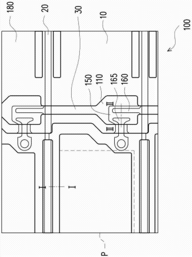
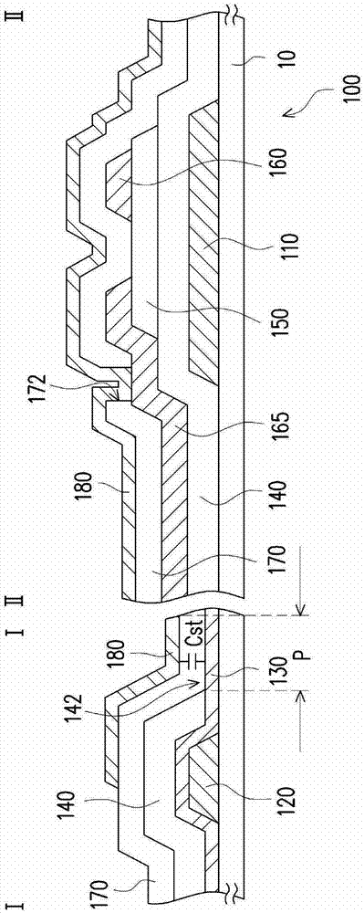
[0041] figure 1 It is a top perspective schematic diagram of a pixel structure according to an embodiment of the present invention. figure 2 shown along figure 1 Schematic cross-sectional view of line I-I and line II-II. Please also refer to figure 1 and figure 2 , in this embodiment, the pixel structure 100 is configured on a substrate 10, wherein the substrate 10 may be a glass substrate, a plastic substrate or a substrate made of other materials. The pixel structure 100 is electrically connected to the scanning line 20 and the data line 30, and the pixel structure 100 includes a gate 110, a capacitor electrode 120, a capacitor transparent electrode 130, a gate insulating layer 140, a semiconductor layer 150, a source 160 , a drain 165 , a protection layer 170 and a pixel electrode 182 .

[0042] In detail, the gate 110 is disposed on the substrate 10 . The capacitor electrode 120 is disposed on the substrate 10 . The capacitive transparent electrode 130 is disposed...


PUM


Abstract

The invention discloses a picture element structure. The picture element structure comprises a gate electrode, a capacitor electrode, a capacitor transparency electrode, a gate insulating layer, a semiconductor layer, a source electrode, a drain electrode, a protective layer and a picture element electrode. The gate electrode and the capacitor electrode are arranged on a substrate in a matched mode. The capacitor transparency electrode covers the capacitor electrode and part of the substrate. The gate insulating layer covers the gate electrode and the capacitor transparency electrode. The gate insulating layer is provided with an opening, wherein part of the capacitor transparency electrode is exposed out of the opening. The source electrode and the drain electrode are exposed out of part of the semiconductor layer. The protective layer covers the source electrode, the drain electrode, the gate insulating layer and the capacitor transparency electrode exposed out of the opening. The protective layer is provided with a contact window, wherein part of the drain electrode is exposed out of the contact window, and the picture element electrode penetrates through the contact window and is in electric connection with the drain electrode. An overlapped area is arranged between the picture element electrode and the capacitor transparency electrode exposed out of the opening to from a storage capacitor.

Description

technical field [0001] The present invention relates to a pixel structure and its manufacturing method, and in particular to a pixel structure with a storage capacitor and its manufacturing method. Background technique [0002] Due to the increasing demand for displays and the rise of the concept of green environmental protection in recent years, thin film transistor liquid crystal displays (thinfilmtransistorliquidcrystaldisplay, TFT-LCD) with superior characteristics such as high image quality, good space utilization efficiency, low power consumption, and no radiation have gradually become The mainstream of the display market. In order to meet the needs of users, the performance of thin film transistor liquid crystal displays is constantly moving towards high contrast (high contrast), no gray scale inversion (no gray scale inversion), small color shift (little color shift), high brightness (high luminance), high color richness, high color Features such as saturation, fast...

Claims


Application Information

Patent Timeline
Patent Type & Authority Patents(China)
IPC IPC(8): H01L27/02H01L29/786H01L21/77G02F1/1362G02F1/1368
Inventor 韩家荣欧李启维陈柏玮许宇禅黄隽尧
Owner HUAYING OPTOELECTRONICS
Why Eureka
Try Eureka