Pixel structure and manufacturing method therefor

A technology of pixel structure and manufacturing method, which is applied in semiconductor/solid-state device manufacturing, photolithographic process exposure device, optics, etc., can solve problems such as cost increase, achieve simplified steps, high storage capacitance value, and reduce production costs.

Inactive Publication Date: 2009-05-06
CHUNGHWA PICTURE TUBES LTD
View PDF7 Cites 0 Cited by
  • Summary
  • Abstract
  • Description
  • Claims
  • Application Information

AI Technical Summary

Problems solved by technology

[0005] This existing pixel structure 100 needs five photomasks to form, but the more photomasks there are, the cost will increase relatively.

Method used


Image

  • Pixel structure and manufacturing method therefor
  • Pixel structure and manufacturing method therefor
  • Pixel structure and manufacturing method therefor

Examples


Embodiment Construction

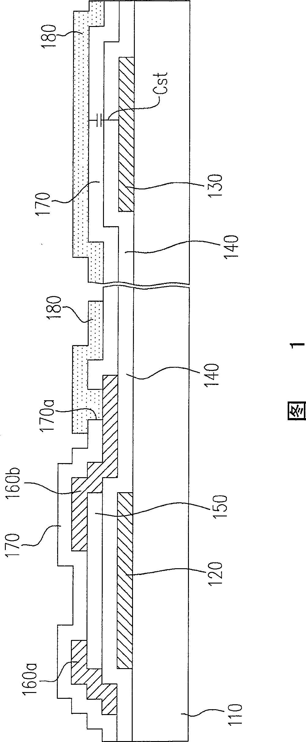
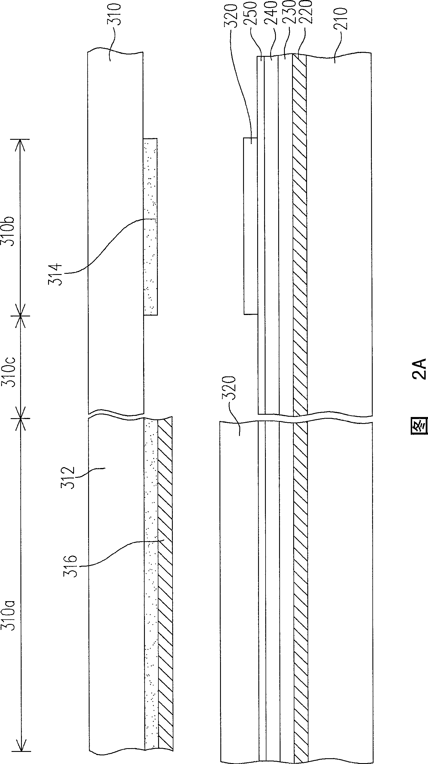
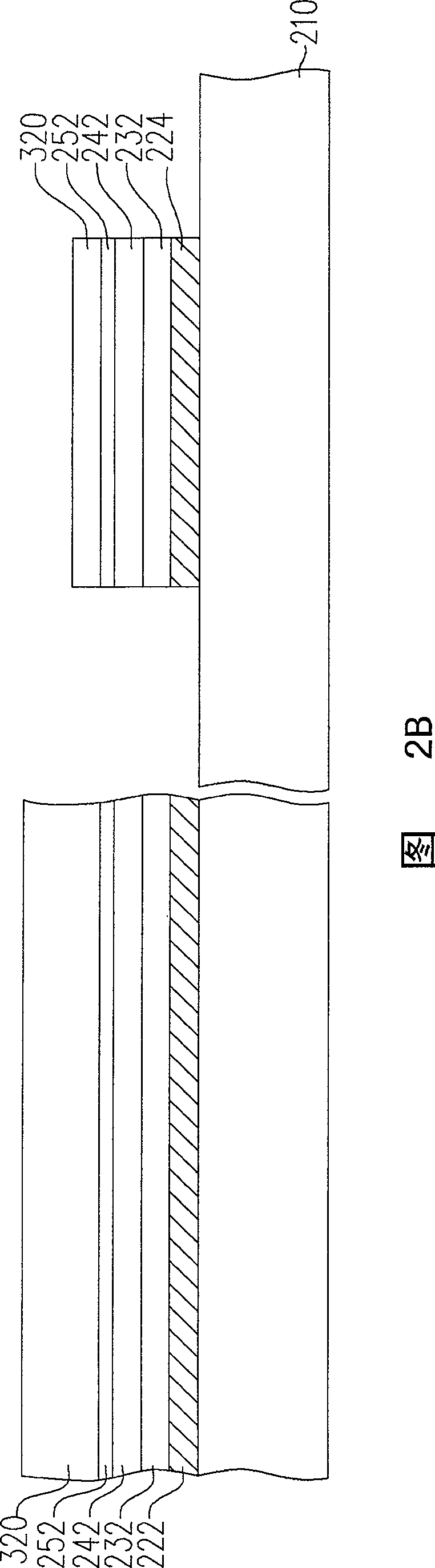
[0056] 2A to 2G are schematic diagrams of a method for manufacturing a pixel structure according to an embodiment of the present invention. Please refer to FIG. 2A , the manufacturing method of the pixel structure in this embodiment includes the following steps. First, a substrate 210 is provided, and a metal layer 220 , a gate insulating layer 230 and a semiconductor material layer 240 are sequentially formed on the substrate 210 . In addition, in order to improve the electrical quality of the device, an ohmic contact material layer 250 may also be formed on the semiconductor material layer 240 .

[0057] Then, a mask 310 is provided, and the mask 310 is, for example, a halftone mask. In addition, the mask 310 includes a transparent substrate 312 , a semi-transmissive film 314 and a light shielding layer 316 . Wherein, the semi-transmissive film 314 is disposed on the transparent substrate 312, and the light-shielding layer 316 is disposed on the semi-transparent film 314, ...


PUM


Abstract

A production method of image structure is provided; a metal layer, a gate insulation layer and a semiconductor material layer are formed in sequence on a substrate. The invention provides a light cover with an opacity area and a light area and forms a patterned light resistance layer on the semiconductor material layer with the help of the light cover. As a cover, the patterned light resistance layer removes partial metal layer, partial gate insulation layer and partial semiconductor material layer to form a gate, a bottom electrode, a patterned gate insulation layer and a semiconductor material layer. Partial patterned light resistance layer is removed to expose the semiconductor layer above the bottom electrode. As a cover, the patterned light resistance layer removes the patterned gate insulation layer and the semiconductor layer above the bottom electrode. The patterned light resistance layer is removed, a source cathode and a drain electrode are formed on the semiconductor layer, a patterned protection layer and a pixel electrode are formed in sequence on the substrate.

Description

technical field [0001] The present invention relates to a pixel structure and its manufacturing method, and in particular to a pixel structure formed by using four photomasks and its manufacturing method. Background technique [0002] The multimedia technology in today's society is quite developed, most of which benefit from the progress of semiconductor elements or display devices. As far as displays are concerned, thin film transistor liquid crystal displays (TFT-LCDs), which have superior characteristics such as high image quality, good space utilization efficiency, low power consumption, and no radiation, have gradually become the mainstream of the market. [0003] A general thin film transistor liquid crystal display is mainly composed of a thin film transistor array substrate, a counter substrate and a liquid crystal layer sandwiched between the two substrates. Wherein, the thin film transistor array substrate mainly includes a substrate, thin film transistors arrayed...

Claims


Application Information

Patent Timeline
Patent Type & Authority Patents(China)
IPC IPC(8): G03F7/20H01L21/00G02F1/136
Inventor 宋慧敏洪孟锋
Owner CHUNGHWA PICTURE TUBES LTD
Why Eureka
Try Eureka