Unlock instant, AI-driven research and patent intelligence for your innovation.

Array substrate, liquid crystal display panel and display device

An array substrate and substrate technology, which is applied in nonlinear optics, instruments, optics, etc., can solve the problems of non-disappearance of liquid crystal display panels and irregular arrangement of liquid crystal molecules, and achieve the effect of improving the display effect.

Active Publication Date: 2016-05-18
BOE TECH GRP CO LTD +1
View PDF6 Cites 1 Cited by
  • Summary
  • Abstract
  • Description
  • Claims
  • Application Information

AI Technical Summary

Problems solved by technology

[0005] The disadvantage of the prior art is that, if figure 2 as shown, figure 2 It is a display effect diagram of a liquid crystal display panel in the prior art. Since the liquid crystal molecules of the pixel unit in the ADS mode liquid crystal display panel 20 are affected by the lateral electric field generated by the data line, the liquid crystal molecules at the edge of the pixel unit are arranged irregularly, When the liquid crystal display panel is subjected to external force (finger pressure / swipe, etc.), the irregular liquid crystal molecules on the edge will drive the arrangement of the liquid crystal molecules in the relatively weaker part of the pixel area to change, and finally appear as indentations on the liquid crystal display panel. Or the phenomenon that scratches do not disappear

Method used


Image

  • Array substrate, liquid crystal display panel and display device
  • Array substrate, liquid crystal display panel and display device
  • Array substrate, liquid crystal display panel and display device

Examples


Embodiment Construction

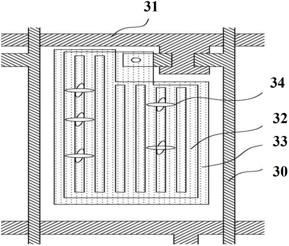
[0031] In order to improve the display effect of a liquid crystal display panel, an embodiment of the present invention provides an array substrate, a liquid crystal display panel and a display device. In the technical solution of the present invention, the two ends of the transparent electrode adopt a bent structure, so that the electric field at both ends of the transparent electrode and the intermediate electric field form a complementary relationship in strength, and the influence of the side electric field formed by the data line on the liquid crystal molecules in the normal display area is blocked. , thereby improving the display effect of the liquid crystal display panel. In order to make the purpose, technical solution and advantages of the present invention clearer, the following examples are given to further describe the present invention in detail.

[0032] Such as image 3 and Figure 4 as shown, image 3 A schematic structural diagram of an array substrate prov...


PUM


Abstract

An array substrate, a liquid crystal display panel (20) and a display device. The array substrate comprises: a substrate (10); a first transparent conductive layer (11) disposed on the substrate (10); an insulating layer (12) disposed on the first conductive layer (11); and a second transparent conductive layer (13) disposed on the insulating layer (20) and configured for forming a horizontal electric field with the first transparent conductive layer (11); the second conductive layer (13) comprises a plurality of transparent electrodes (14), adjacent transparent electrodes (14) possess a slit structure therebetween, and two ends of each transparent electrode each possess a bent structure (16).

Description

technical field [0001] The invention relates to the technical field of liquid crystal display, in particular to an array substrate, a liquid crystal display panel and a display device. Background technique [0002] Among flat panel display devices, Thin Film Transistor Liquid Crystal Display (TFT-LCD) has the characteristics of small size, low power consumption, relatively low manufacturing cost and no radiation, and occupies a dominant position in the current flat panel display market. At present, the display modes of TFT-LCD mainly include TN (TwistedNematic, twisted nematic) mode, VA (VerticalAlignment, vertical orientation) mode, IPS (In-PlaneSwitching, plane direction conversion) mode and AD-SDS (ADvancedSuperDimensionSwitch, advanced ultra-dimensional field conversion, referred to as ADS) mode, etc. [0003] Among them, the ADS mode is the core technology of planar electric field wide viewing angle - Advanced SuperDimension Switching technology (ADvancedSuperDimension...

Claims


Application Information

Patent Timeline
Patent Type & Authority Patents(China)
IPC IPC(8): G02F1/1343
CPCG02F1/133707G02F1/134363G02F1/134318G02F1/133345G02F1/13439
Inventor 张洪林赵合彬刘莎王丹
Owner BOE TECH GRP CO LTD