
Magnetic nanowire array thin film and preparation method thereof
A magnetic nanometer and line array technology, applied in ion implantation plating, metal material coating process, coating, etc., to meet the needs of different operating frequencies, simple operation, and good insulation
- Summary
- Abstract
- Description
- Claims
- Application Information
AI Technical Summary
Problems solved by technology
Method used
Image

Examples
Embodiment Construction
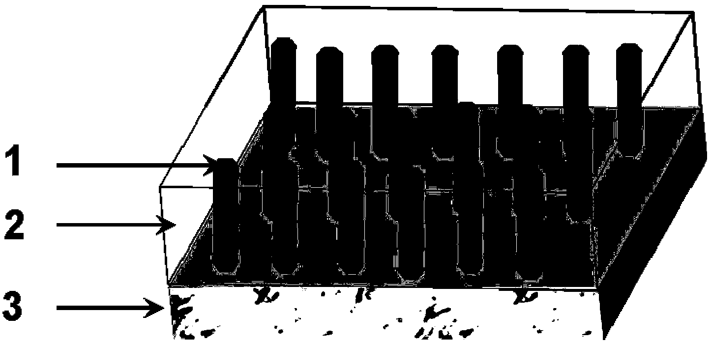
[0035] A magnetic nanowire array thin film, such as figure 1 shown, including MgAl 2 o 4 (MAO) single crystal substrate 3, Pb(Zr 0.52 Ti 0.48 )O 3 (PZT) matrix 2 and NiFe 2 o 4 (NFO) nanowires1. Among them, the MgAl 2 o 4 (MAO) single crystal substrate 3 is (001) oriented and surface polished MgAl 2 o 4 single crystal substrate; the NiFe 2 o 4 The nanowires 1 are uniformly distributed in Pb(Zr 0.52 Ti 0.48 )O 3 In the substrate 2, a magnetic nanowire array film is formed; the magnetic nanowire array film is deposited on the MgAl 2 o 4 (MAO) on the (001) oriented surface of the single crystal substrate 3 .
[0036] Further, the NiFe 2 o 4 The diameter of the nanowire 1 is between 70nm and 250nm, and the length is between tens of nanometers and several microns.
[0037] In the magnetic nanowire array thin film provided by the invention, the PZT substrate has high insulation and piezoelectricity at the same time, and the NFO nanostructure has high insulation, ...
PUM
| Property | Measurement | Unit |
|---|---|---|
| diameter | aaaaa | aaaaa |
| diameter | aaaaa | aaaaa |
| thickness | aaaaa | aaaaa |
Abstract
Description
Claims
Application Information