band pass filter

A band-pass filter and microstrip technology, applied in waveguide-type devices, electrical components, circuits, etc., can solve the problems of filter influence, increase of filter plane area and insertion loss, and difficulty in reducing size.

Active Publication Date: 2015-12-09
SHENZHEN INST OF ADVANCED TECH CHINESE ACAD OF SCI
View PDF2 Cites 0 Cited by
  • Summary
  • Abstract
  • Description
  • Claims
  • Application Information

AI Technical Summary

Problems solved by technology

The coupling of two adjacent resonators in the filter is necessary, but the coupling between non-adjacent resonators (also called parasitic coupling) still exists, and this parasitic coupling will have an adverse effect on the filter
A common solution is to add a low-pass filter, but this will lead to a further increase in filter planar area and insertion loss
[0007] Therefore, it is difficult to further reduce the size of the traditional filter structure

Method used


Image

  • band pass filter
  • band pass filter
  • band pass filter

Examples


Embodiment 1

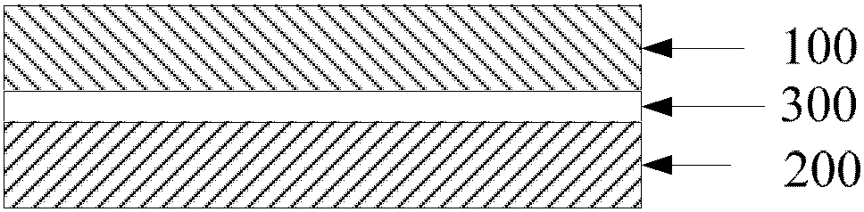
[0053] by figure 2 The defect ground structure shown and Figure 7 The shown double spiral microstrip structure is respectively used as the first layer and the second layer of the bandpass filter, and a dielectric layer is set at the first layer and the second layer.

[0054] The specific parameters of the defect ground structure and the double helix microstrip structure are as follows:

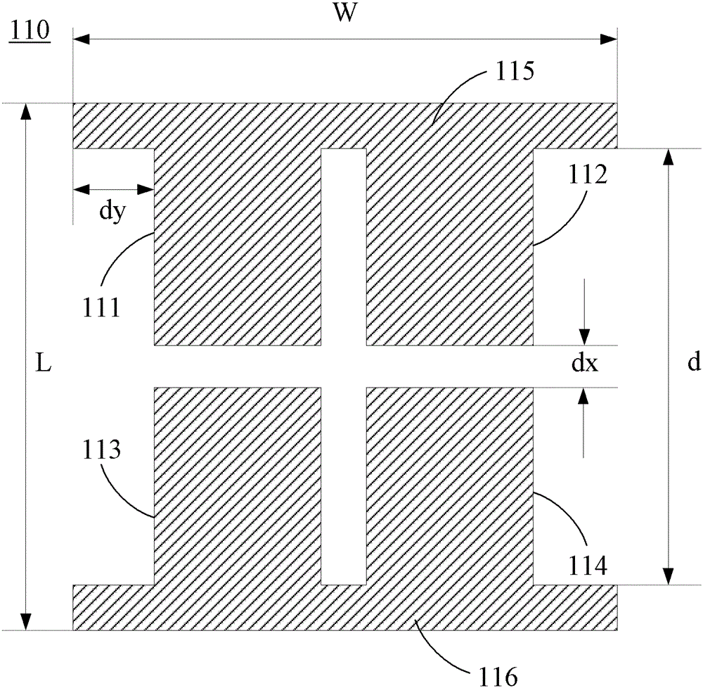
[0055] The overall length of the defective ground structure is L=4.3mm, and the overall width is W=4.3mm; the four blocky areas are equidistantly distributed, with a distance of dx=0.2mm and a distance of dy=1.34mm, between the microstrip lines at two opposite edges The distance d=3.4mm. The defective structure is made of copper.

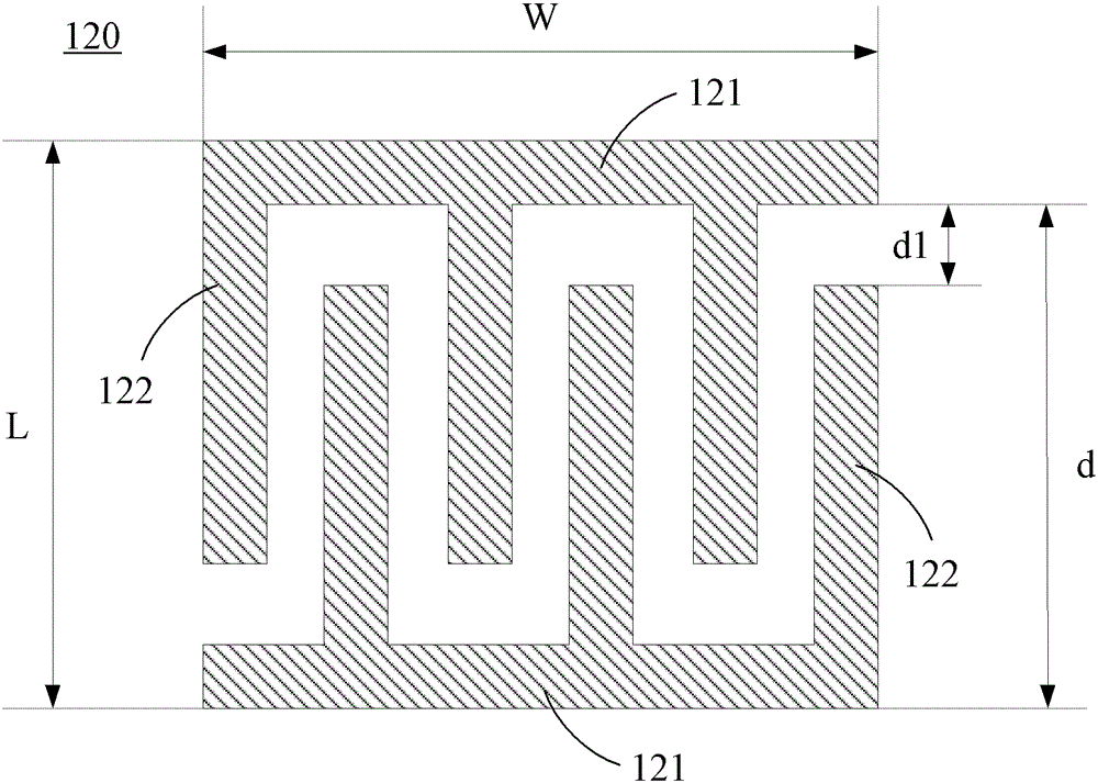
[0056] The overall length of the double-helix microstrip structure is L=4.3mm, and the overall width is W=4.3mm; the width of all microstrip lines is w=0.16mm, the line spacing is g=0.1mm, and the distance between ports 231 is z=0.8mm.

[0057] The dielectric ...

Embodiment 2

[0061] by image 3 The defect ground structure shown and Figure 7 The shown double spiral microstrip structure is respectively used as the first layer and the second layer of the bandpass filter, and a dielectric layer is set at the first layer and the second layer.

[0062] The specific parameters of the defect ground structure and the double helix microstrip structure are as follows:

[0063] The overall length of the defective ground structure L=4.95mm, the overall width W=4.78mm; the distance between the end of the comb tooth microstrip line and the comb ridge d1=0.5mm, the distance between the comb ridge d=3.5mm, the distance between the comb teeth The spacing between: 0.02mm ~ 0.1mm. The defective structure is made of copper.

[0064] The overall length of the double helix microstrip structure L=4.3mm, the overall width W=4.3mm; the width of all microstrip lines w=0.2mm, the line spacing g1=g12=0.02~0.06mm, g2=...g11= 0.12-0.2 mm, the distance z between ports 231 is...

Embodiment 3

[0068] by Figure 4 The defect ground structure shown and Figure 7 The shown double spiral microstrip structure is respectively used as the first layer and the second layer of the bandpass filter, and a dielectric layer is set at the first layer and the second layer.

[0069] The specific parameters of the defect ground structure and the double helix microstrip structure are as follows:

[0070] The comb-line cross-coupled microstrip structure is used. This structure can make the electric field mainly concentrate in the finger capacitance during resonance, forming a strong electric field effect, just like a large resistor in series, which improves the impedance of the system. The center frequency continues to move towards the low frequency direction. The defective structure is made of copper.

[0071] Double-helix microstrip structure microstrip line width w=0.02mm~0.3mm is consistent, line spacing g1=g12=0.02mm~0.1mm, g2=g3=......=g11=0.02mm~0.1mm; gm1=gm10=0.02˜0.2 mm, ...


PUM


Abstract

Disclosed is a band-pass filter, comprising a first layer which is in a ground structure containing defects, a second layer which is in a double helix microstrip structure, and a dielectric layer which is arranged between the first layer and the second layer. The first layer is coupled to the second layer to form a capacitor. Using the ground structure containing defects and the double helix microstrip structure enables the plane dimension of the overall filter to not be more than 10 mm × 10 mm on the premise of maintaining the normal filter function, thereby solving the problem of miniaturization of passive band-pass filters.

Description

【Technical field】 [0001] The present invention relates to electronic circuits, in particular to a band-pass filter. 【Background technique】 [0002] The rapid development of wireless communication technology and integrated circuit technology has put forward higher technical requirements for communication electronic equipment, that is, high integration and miniaturization. High-density packaging technologies such as 3-dimensional through-silicon via (3D-TSV) and system-in-package (SiP) can reduce the substrate area of ​​the system to a certain extent. However, as the system integration level continues to increase, due to the slow speed of miniaturization of passive devices, the area of ​​the system substrate occupied by passive devices will become larger and larger. [0003] Passive band-pass filters are widely used in the field of communication as an important component of communication terminals. Usually, the size of such passive band-pass filters is relatively large, espec...

Claims


Application Information

Patent Timeline
Patent Type & Authority Patents(China)
IPC IPC(8): H01P1/203
CPCH01P1/203H01P1/20336
Inventor 孙蓉于淑会杨文虎杜如虚
Owner SHENZHEN INST OF ADVANCED TECH CHINESE ACAD OF SCI
Why Eureka
Try Eureka