
A wafer testing method

A wafer testing and wafer technology, applied in the field of wafer testing, can solve the problems of chip defects, testing, bad test results, etc., and achieve the effect of improving efficiency

Active Publication Date: 2013-10-02
SHANGHAI HUAHONG GRACE SEMICON MFG CORP
View PDF6 Cites 12 Cited by
  • Summary
  • Abstract
  • Description
  • Claims
  • Application Information

AI Technical Summary

Problems solved by technology

[0006] The present invention provides a wafer test method to solve the problem that the prior art cannot directly distinguish whether the bad test result is due to the fact that the chip is actually defective or caused by the test

Method used


Image

  • A wafer testing method
  • A wafer testing method
  • A wafer testing method

Examples


Embodiment 1

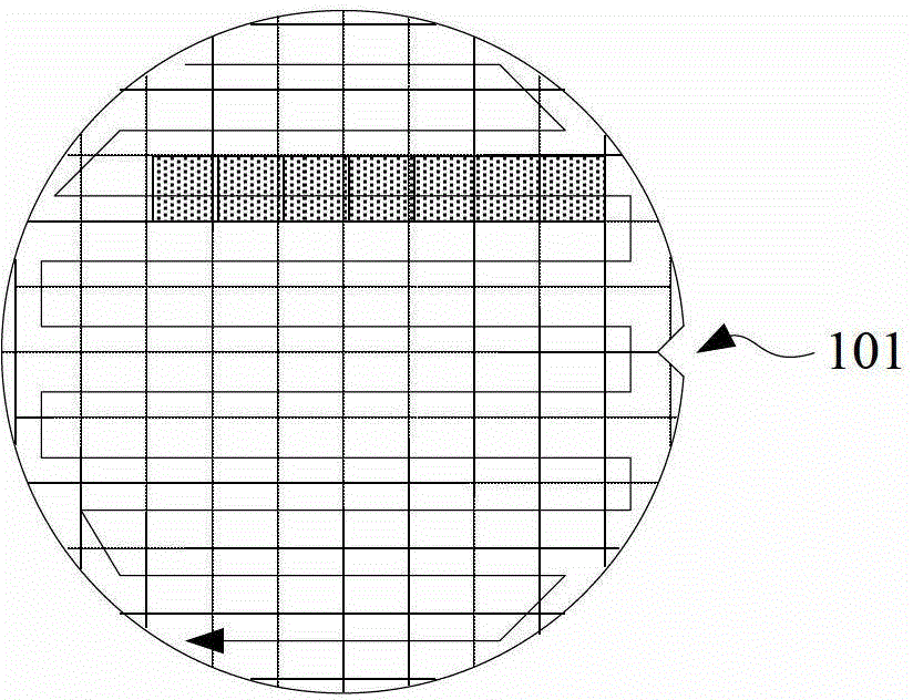
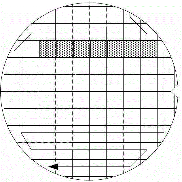
[0023] The wafers to be tested are multiple wafers of the same product in the same batch, for example, a box of wafers (25 pieces) in standard production, and the multiple wafers are divided into two groups, and these two groups The testing directions of the wafers are perpendicular to each other. If there is an influence of the test itself, there will be obvious differences on the wafers tested in different directions, so as to directly distinguish whether there is a problem in the test itself.

[0024] Preferably, the odd-numbered wafers and the even-numbered wafers are divided into two groups, and the odd-numbered wafers are tested in the first direction; the even-numbered wafers in the plurality of wafers are tested in the first direction perpendicular to the first direction. Test in two directions. better, see Figure 2A to Figure 2B , define the direction of the diameter of the wafer notch and the center of the wafer (the horizontal direction in the figure) as the firs...

Embodiment 2

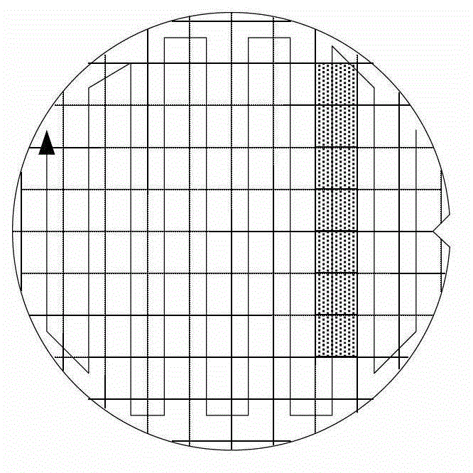
[0028] In this embodiment, the wafer to be tested is a single wafer, and different regions on the wafer are tested in two mutually perpendicular directions on the wafer to be tested respectively, and the test results can be identified through the test results. Whether the resulting yield distribution is affected by the test issue.

[0029] Specifically, in this embodiment, the wafer is divided into four regions by two mutually perpendicular chords on the wafer, and the directions in which two adjacent regions are tested are perpendicular to each other. Preferably, the wafer is equally divided into four regions by using two mutually perpendicular diameters on the wafer. In this embodiment, one of the diameters is selected as the diameter passing through the wafer notch, such as image 3 shown. These four regions are defined clockwise as the first region 311, the second region 312, the third region 313, and the fourth region 314; The direction perpendicular to the first direct...


PUM


Abstract

The invention provides a wafer testing method. The wafer testing method carries out a test on a to-be-tested wafer respectively along two directions which are mutually perpendicular. When the wafer test is influenced by factors of the test itself, test results in different directions can present obvious distinguishable distributions, so that whether yield rate distributions are influenced by factors of the test itself can be identified directly according to the test results, and the production efficiency is substantially raised.

Description

technical field [0001] The invention relates to the field of integrated circuit manufacturing, in particular to a wafer testing method. Background technique [0002] Wafer testing (Chip Probing, CP) is to test the electrical capability and circuit function of each chip on the wafer after the wafer manufacturing is completed. Wafer test is also called die sort or wafer sort. [0003] Wafer testing is for the following purposes. First, before the wafer is sent to the packaging factory, qualified chips can be identified, and unqualified chips will not be packaged in the subsequent process to save costs. In addition, the electrical parameters of the device / circuit can be evaluated, and engineers can control the quality level of the process through the distribution status of these monitoring parameters. [0004] During testing, the wafer is held on a vacuum-suction chuck while probes are in contact with each pad of the chip. The tester inputs current or voltage into the device...

Claims


Application Information

Patent Timeline
Patent Type & Authority Applications(China)
IPC IPC(8): G01R31/28
Inventor 王善屹王磊
Owner SHANGHAI HUAHONG GRACE SEMICON MFG CORP
Learn More