Electron microscope analysis method for defect detection according to circuit pattern

An electron microscope and defect detection technology, which is used in material analysis, material analysis, and measurement devices using wave/particle radiation. The effect of improving the effective operation efficiency

Active Publication Date: 2015-07-08
SHANGHAI HUALI MICROELECTRONICS CORP
View PDF13 Cites 0 Cited by
  • Summary
  • Abstract
  • Description
  • Claims
  • Application Information

AI Technical Summary

Problems solved by technology

[0007] In view of the above-mentioned problems, the present invention discloses an electron microscope analysis method for defect detection according to circuit patterns, so as to overcome the problems in the prior art that the electron microscope repeatedly photographs and compares different chips, resulting in low efficiency of the effective operation of the equipment, and when relatively The problem that the defect capture will fail when adjacent chips also have duplicate defects

Method used


Image

  • Electron microscope analysis method for defect detection according to circuit pattern
  • Electron microscope analysis method for defect detection according to circuit pattern
  • Electron microscope analysis method for defect detection according to circuit pattern

Examples


Embodiment Construction

[0023] The present invention will be further described below in conjunction with the accompanying drawings and specific embodiments, but not as a limitation of the present invention.

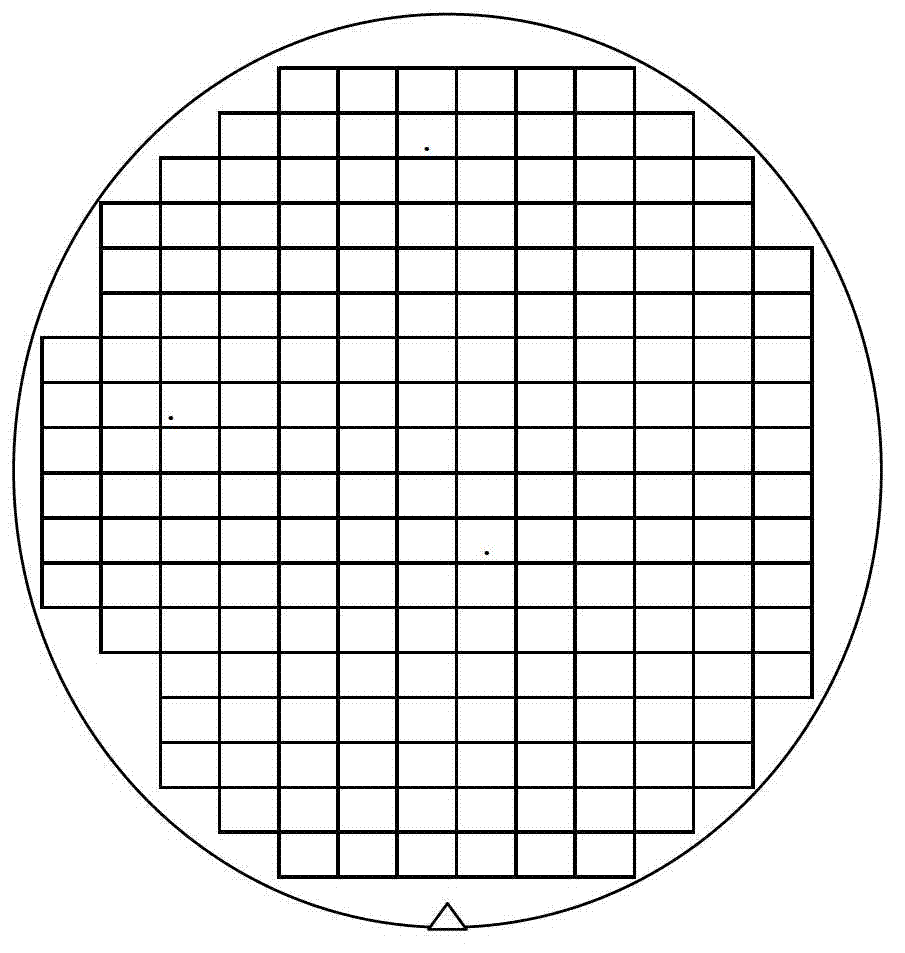
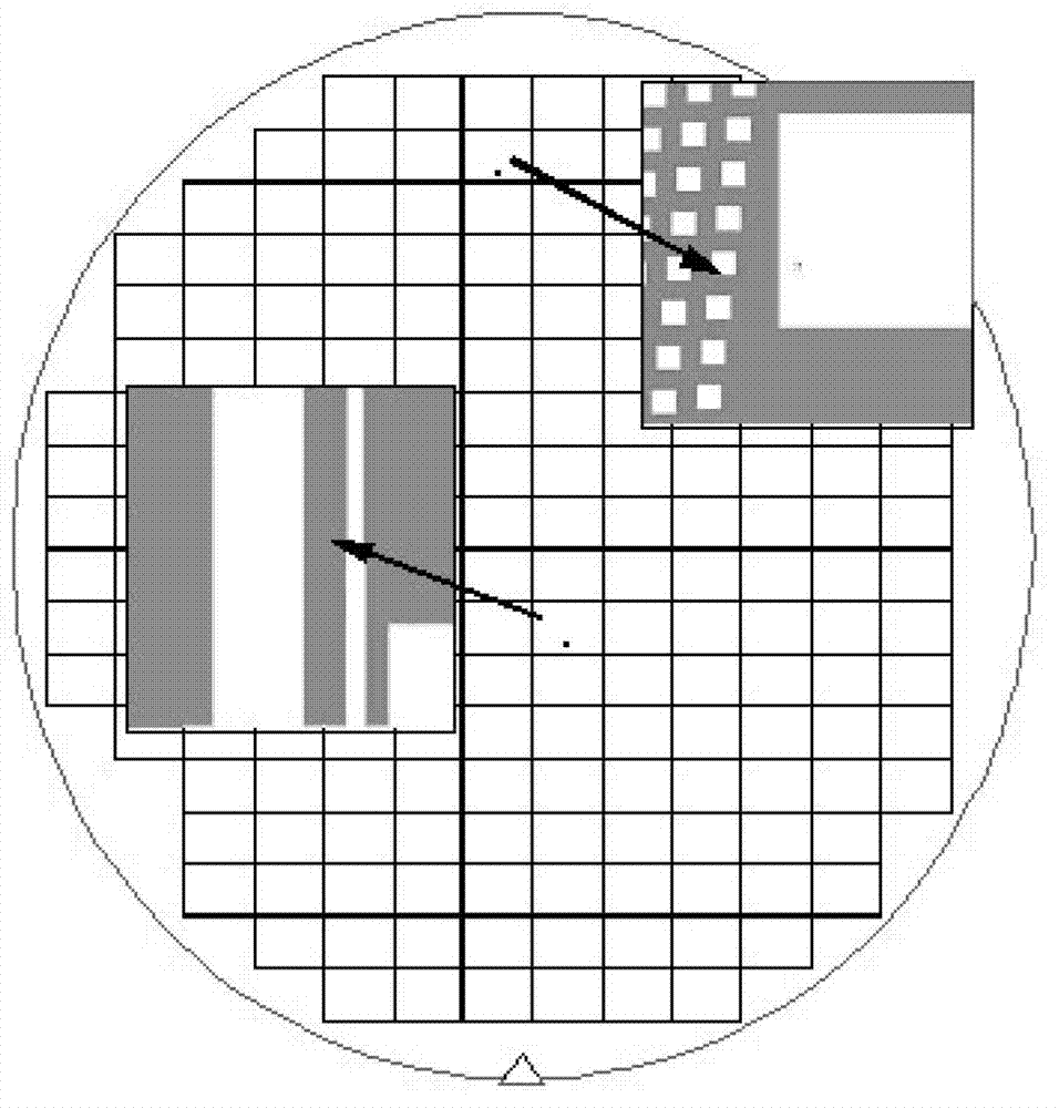
[0024] In the prior art, when the defect inspection equipment scans the wafer for defects, it will obtain the coordinates of the defects generated in the process according to the chip comparison data. For example, the first defect: (x1, y1); the second defect Defects: (x2, y2) etc. However, when the coordinates of these defects are transmitted to the electron microscope for observation, due to the difference between the two devices, the coordinate positions of (x1, y1) and (x2, y2) cannot be directly passed Find bugs.

[0025] As an embodiment of the present invention, this embodiment relates to an electron microscope analysis method for detecting defects according to circuit patterns, which is applied to the defect detection and analysis process of wafers, and the chip design circuit patterns i...


PUM


Abstract

The invention discloses an electron microscope analysis method for defect detection according to a circuit pattern. The method comprises the following steps: selecting the characteristic circuit pattern of a chip design circuit pattern; inputting a defect location file scanned by defect detection equipment into a server, and converting the defect location file into a defect file with the characteristic circuit pattern through the server; guiding the defect file into an electron microscope; and comparing the characteristic circuit pattern of the defect file to determine a defect location through the electron microscope. According to the technology of the method, the electron microscope compares the characteristic circuit pattern of the defect file to determine the defect location and take photos, the step of constantly taking photos at adjacent chips is removed, the effective operation efficiency of the equipment is greatly increased, and meanwhile the capture failure of repeat defects of the adjacent chips can be avoided.

Description

technical field [0001] The invention relates to the technical field of integrated circuit manufacturing, in particular to an electron microscope analysis method for defects on a wafer, in particular to an electron microscope analysis method for defect detection according to circuit patterns. Background technique [0002] The manufacturing process of integrated circuits is very complicated. Simply put, it is to use various methods to form different "layers" on the substrate material (such as silicon substrate), and to dope ions in selected areas to change the semiconductor material. Conductive properties, the process of forming semiconductor devices. This process requires many steps to complete, and it takes about hundreds of processes from wafer to finished integrated circuit, especially the more advanced processes involve more processes. Through this complicated process one by one, thousands or even hundreds of millions of transistors can be integrated on a tiny chip. This...

Claims


Application Information

Patent Timeline
Patent Type & Authority Patents(China)
IPC IPC(8): G01N23/225H01L21/66
Inventor 倪棋梁陈宏璘龙吟王恺
Owner SHANGHAI HUALI MICROELECTRONICS CORP
Why Eureka
Try Eureka