Touch panel

A touch panel and substrate technology, applied in the direction of instrument, electrical digital data processing, data processing input/output process, etc., can solve the problems of not easy to large-scale, heavy PCB board, high cost, easy to achieve thickness and size, The effect of low cost and easy upsizing

Inactive Publication Date: 2013-12-18
TIANJIN FUNA YUANCHUANG TECH +1
View PDF4 Cites 3 Cited by
  • Summary
  • Abstract
  • Description
  • Claims
  • Application Information

AI Technical Summary

Problems solved by technology

However, for some small household appliances, toys, and keyboards and other fields, PCB boards are used to build touch panels, and the cost is relatively high.
In addition, large-sized PCB boards are relatively thick, so traditional non-penetrating touch panels are not easy to make larger, that is, it is not easy to be large-sized

Method used


Image

  • Touch panel
  • Touch panel
  • Touch panel

Examples


Embodiment Construction

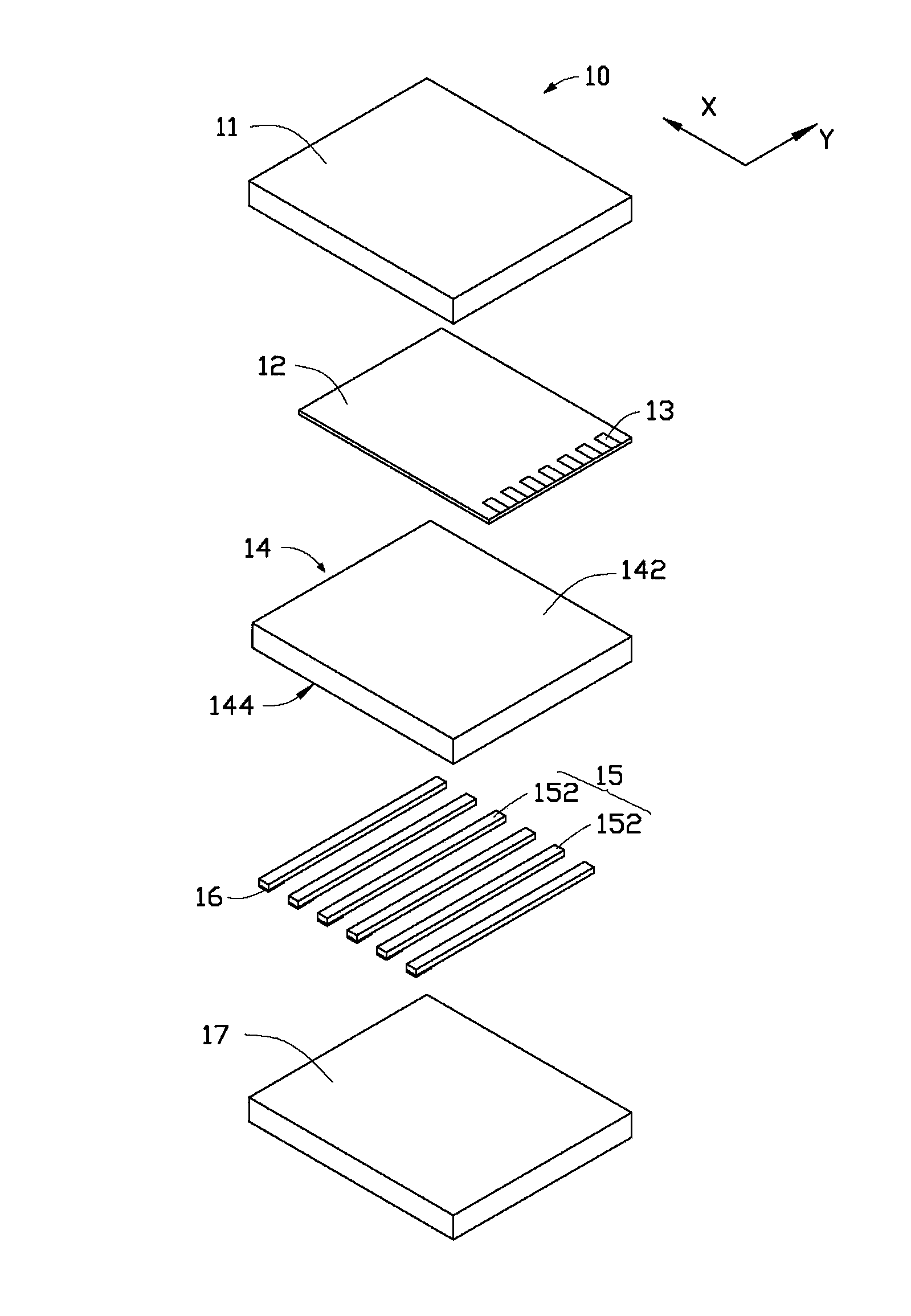
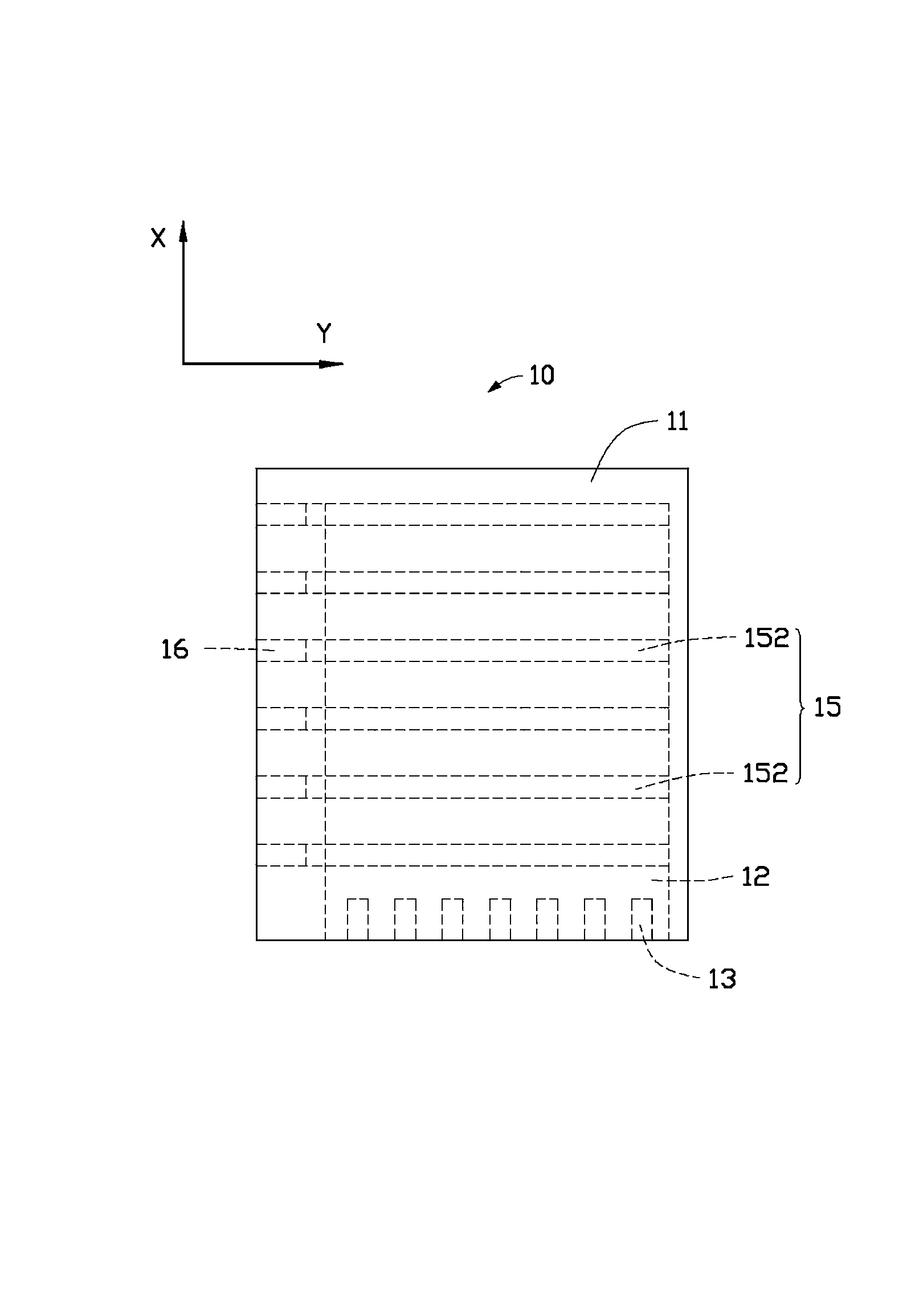
[0015] see figure 1 and figure 2 , the first embodiment of the present invention provides a touch panel 10, the touch panel 10 is a non-penetrating touch panel. The touch panel 10 includes a first conductive layer 12 , a plurality of first electrodes 13 , an insulating layer 14 , a second conductive layer 15 and a plurality of second electrodes 16 . Wherein, the first conductive layer 12 , the insulating layer 14 , and the second conductive layer 15 are sequentially stacked. The plurality of first electrodes 13 are spaced apart from each other and electrically connected to the first conductive layer 12 . The plurality of second electrodes 16 are spaced apart from each other and electrically connected to the second conductive layer 15 .

[0016] The insulating layer 14 has a first surface 142 and a second surface 144 , and the second surface 144 is opposite to the first surface 142 . The first conductive layer 12 is disposed on the first surface 142 of the insulating layer...


PUM

PropertyMeasurementUnit
Thicknessaaaaaaaaaa

Abstract

The invention relates to a touch panel. The touch panel comprises a first conducting layer, an insulating layer and a second conducting layer. The first conducting layer is a carbon nano tube layer, the carbon nano tube layer comprises a plurality of carbon nano tubes, and the plurality of carbon nano tubes extend along a first direction; the second conducting layer comprises a plurality of metal strips, the plurality of metal strips extend along a second direction and are arranged at intervals along the first direction, and the second direction and the first direction are crossed.

Description

technical field [0001] The invention relates to a touch panel, in particular to a touch panel based on carbon nanotubes. Background technique [0002] In recent years, touch technology has been applied and developed in electronic equipment such as computers, mobile phones, home appliances, and toys. Since the electronic equipment adopting the touch technology is easy to use, the touch technology has increasingly become a preferred way of use in people's life. [0003] In terms of light transmission, the touch panel can be mainly divided into a transmissive touch panel that can transmit light and a non-transmissive touch panel that cannot transmit light. Wherein, the non-penetrating touch panel in the prior art usually uses a printed circuit board (PCB board) to achieve the purpose of being touchable. However, for some fields such as small household appliances, toys, and keyboards, PCB boards are used to construct touch panels, and the cost is relatively high. In addition,...

Claims


Application Information

Patent Timeline
IPC IPC(8): G06F3/041
Inventor 赵志涵施博盛郑嘉雄
Owner TIANJIN FUNA YUANCHUANG TECH
Why Eureka
Try Eureka