A method for pretreating a substrate in a carbon-based semiconductor device fabrication process
What is AI technical title?
AI technical title is built by Patsnap AI team. It summarizes the technical point description of the patent document.
A preparation process and semiconductor technology, applied in the field of nanoelectronics, can solve the problems such as the decrease of the carrier mobility of carbon-based materials and the degradation of device performance, and achieve the effect of good repeatability and simple process
Active Publication Date: 2017-03-29
INST OF MICROELECTRONICS CHINESE ACAD OF SCI
View PDF4 Cites 0 Cited by
Summary
Abstract
Description
Claims
Application Information
AI Technical Summary
This helps you quickly interpret patents by identifying the three key elements:
Problems solved by technology
Method used
Benefits of technology
Problems solved by technology
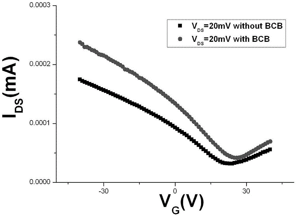
[0006] In view of this, the main purpose of the present invention is to provide a method for pretreating the substrate in the preparation process of carbon-based semiconductor devices, so as to solve the problem of the decrease of the carrier mobility of the carbon-based material transferred to the surface of the target substrate and the The problem of performance degradation
Method used
Image
Click on the blue label to locate the original text in one second.
Reading with bidirectional positioning of images and text.
Examples
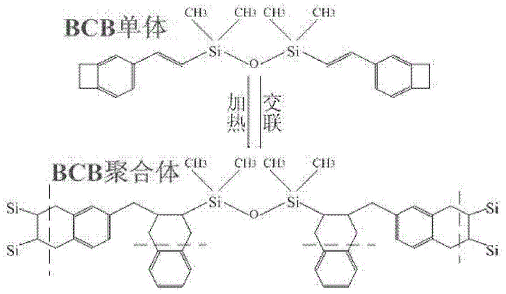
Embodiment 1
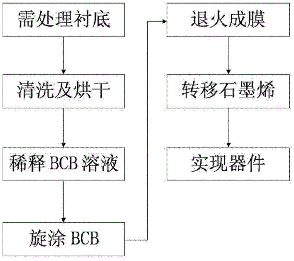
[0029] Embodiment 1: Graphene material is grown by CVD, and a graphene field effect transistor is realized on a silicon dioxide / silicon substrate pretreated by a BCB organic film layer.
[0030] figure 2 Use BCB organic film layer to carry out the flowchart of surface pretreatment to substrate for the present invention, comprise the following steps:
[0031] Step 1: Put the cleaned silicon dioxide / silicon substrate with a thickness of 100nm into an oven at 80°C to 200°C for drying treatment for 5 minutes to 60 minutes;
[0032] Step 2: Prepare a benzocyclobutene (BCB) solution, dilute the BCB solution with an organic solution, and spin-coat the diluted BCB solution on the surface of the substrate through a homogenizer;
[0033] In this example, BCB (Cyclotene 3022-46, purchased from Dow Chemical Company of the United States) and 1,3,5-trimethylbenzene solution are diluted at a volume ratio of 1:27. Spin coating on the surface of the substrate, the speed of the homogenizer i...
Embodiment 2
[0039]Embodiment 2: Graphene material is grown by CVD, and a graphene field effect transistor is realized on a silicon dioxide / silicon substrate pretreated by rapid thermal annealing BCB.
[0040] The specific steps are similar to those in Example 1, but step 3 uses rapid thermal annealing (RTA) to treat the BCB. The BCB is subjected to rapid thermal annealing at 290 degrees Celsius for 15 seconds to form an organic dielectric layer with a thickness of 10 nm.
Embodiment 3
[0041] Embodiment 3: Use micromachines to exfoliate graphene materials, and realize graphene field effect transistors on silicon dioxide / silicon substrates pretreated by BCB.
[0042] The specific steps are similar to those in Example 1, but in Step 4, the micromechanically exfoliated graphene film is transferred to a silicon dioxide / silicon substrate pretreated by BCB, and then a field effect transistor device is realized.
PUM
Abstract
The invention discloses a method for pre-processing a substrate in a carbon-based semiconductor device manufacturing technology. The method comprises the steps that the washed substrate is placed in a drying oven, and drying processing is carried out on the substrate at 80 DEG C-200 DEG C for 5-60 minutes; BCB solutions are prepared, and are diluted through organic solutions, and the diluted BCB solutions coat the surface of the substrate in a spinning mode through a spin coater; under the protection of N2 or inert gas, the substrate with the surface coated with the BCB solutions in the spinning mode is heated to be 200 DEG C-400 DEG C, a cross-linking reaction occurs to benzocyclobutene monomers to generate a benzocyclobutene polymer, and therefore a BCB organic film layer is formed on the surface of the substrate. The method solves the problem that due to the fact that the surface of an original substrate is scattering in polarity, rough and fluctuant and impurity absorption occurs, the performance depredation of a grapheme device occurs, the BCB organic film passivates and decorates the surface of the original substrate, and meanwhile carrier mobility degeneration of grapheme cannot be caused.
Description
technical field [0001] The invention relates to a carbon material-based semiconductor device preparation process, in particular to a method for pretreating a substrate in the carbon-based semiconductor device preparation process, and belongs to the technical field of nanoelectronics. Background technique [0002] Nanoelectronics based on carbon materials, especially those based on carbon nanotubes (Carbon Nanotube) and graphene (Graphene), are considered to have great application prospects and great potential to replace silicon-based materials . Since the successful development of carbon nanotubes in 1991 and graphene in 2004, carbon-based electronics has made great progress. Carbon-based electronics have attracted more and more attention because of their small size, high speed, low power consumption, and simple process. [0003] For carbon-based semiconductor devices, since the conductive carbon material is only one or a few atomic layers thick, it has an important featur...
Claims
Application Information
Patent Timeline
Application Date:The date an application was filed.
Publication Date:The date a patent or application was officially published.
First Publication Date:The earliest publication date of a patent with the same application number.
Issue Date:Publication date of the patent grant document.
PCT Entry Date:The Entry date of PCT National Phase.
Estimated Expiry Date:The statutory expiry date of a patent right according to the Patent Law, and it is the longest term of protection that the patent right can achieve without the termination of the patent right due to other reasons(Term extension factor has been taken into account ).
Invalid Date:Actual expiry date is based on effective date or publication date of legal transaction data of invalid patent.

