Method for pre-processing substrate in carbon-based semiconductor device manufacturing technology

A preparation process and semiconductor technology, applied in the field of nanoelectronics, can solve the problems of carbon-based material carrier mobility decline, device performance degradation, etc., and achieve the effect of good repeatability and simple process

Active Publication Date: 2013-12-18
INST OF MICROELECTRONICS CHINESE ACAD OF SCI
View PDF4 Cites 2 Cited by
  • Summary
  • Abstract
  • Description
  • Claims
  • Application Information

AI Technical Summary

Problems solved by technology

[0006] In view of this, the main purpose of the present invention is to provide a method for pretreating the substrate in the preparation process of carbon-based semiconductor devices, so as to solve the problem of the decrease of the carrier mobility of the carbon-based material transferred to the surface of the target substrate and the The problem of performance degradation

Method used


Image

  • Method for pre-processing substrate in carbon-based semiconductor device manufacturing technology
  • Method for pre-processing substrate in carbon-based semiconductor device manufacturing technology
  • Method for pre-processing substrate in carbon-based semiconductor device manufacturing technology

Examples


Embodiment 1

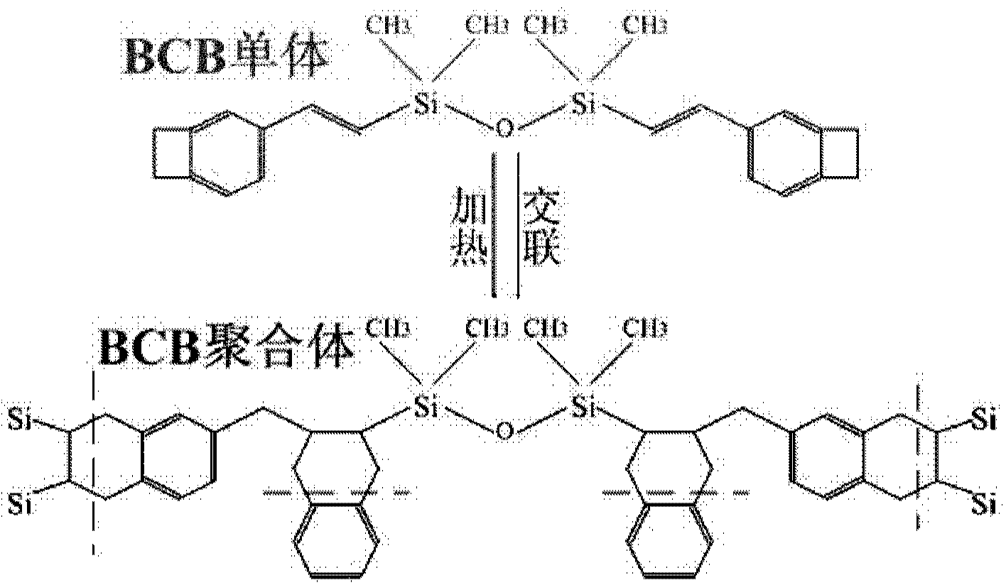
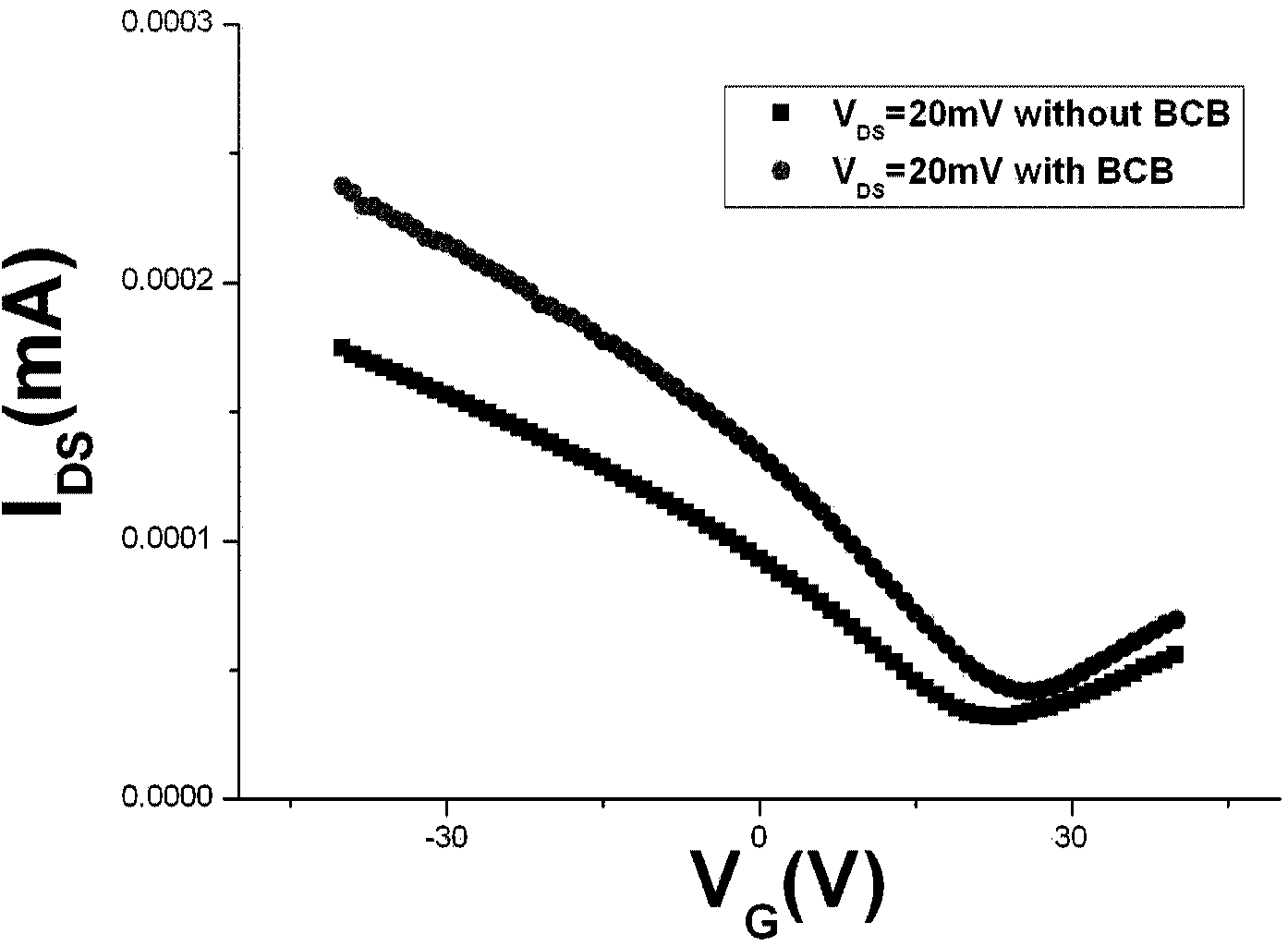
[0029] Embodiment 1: Graphene material is grown by CVD, and a graphene field effect transistor is realized on a silicon dioxide / silicon substrate pretreated by a BCB organic film layer.

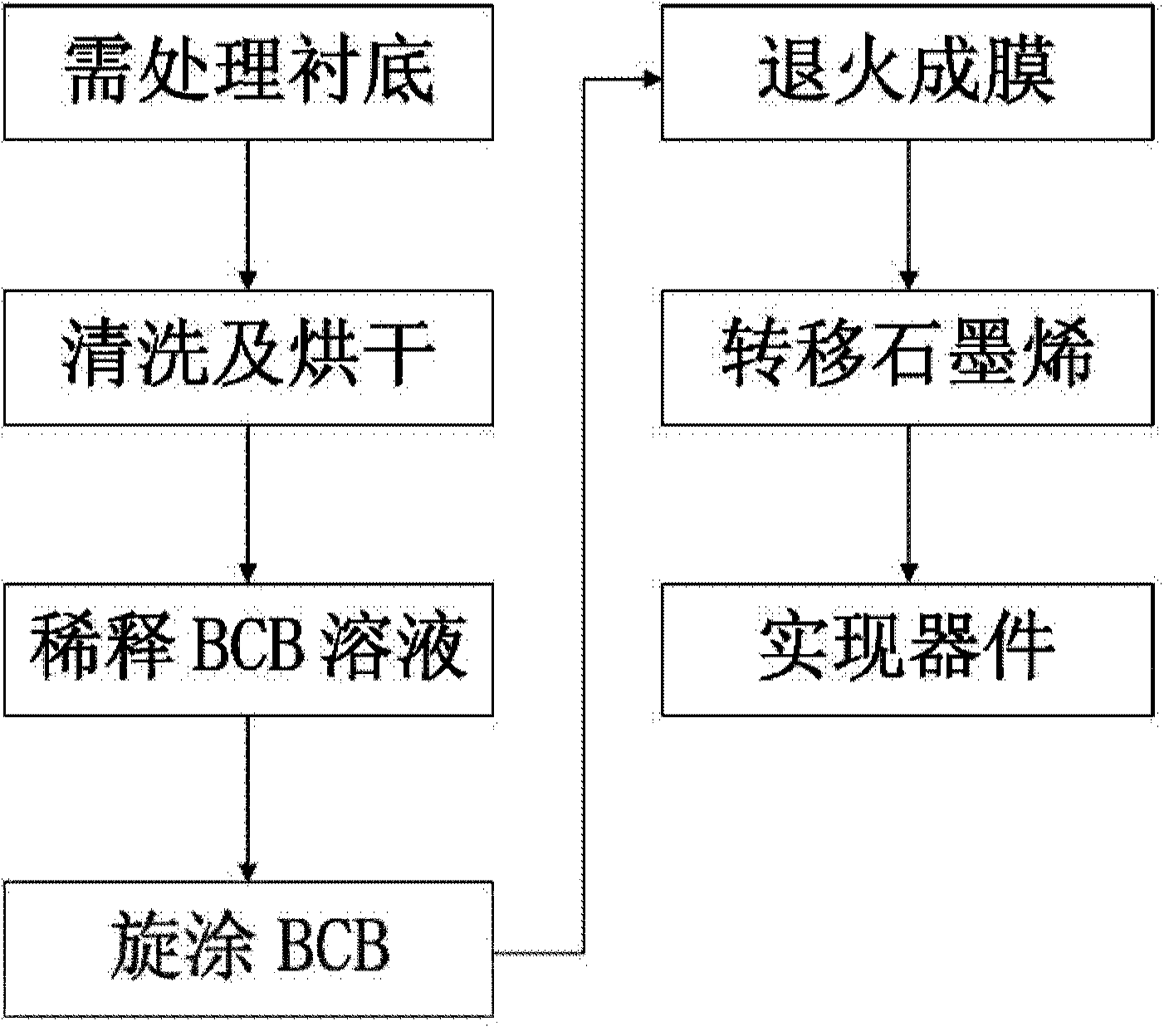
[0030] figure 2 Use BCB organic film layer to carry out the flowchart of surface pretreatment to substrate for the present invention, comprise the following steps:

[0031] Step 1: Put the cleaned silicon dioxide / silicon substrate with a thickness of 100nm into an oven at 80°C to 200°C for drying treatment for 5 minutes to 60 minutes;

[0032] Step 2: Prepare a benzocyclobutene (BCB) solution, dilute the BCB solution with an organic solution, and spin-coat the diluted BCB solution on the surface of the substrate through a homogenizer;

[0033] In this example, BCB (Cyclotene 3022-46, purchased from Dow Chemical Company of the United States) and 1,3,5-trimethylbenzene solution are diluted at a volume ratio of 1:27. Spin coating on the surface of the substrate, the speed of the homogenizer i...

Embodiment 2

[0039]Embodiment 2: Graphene material is grown by CVD, and a graphene field effect transistor is realized on a silicon dioxide / silicon substrate pretreated by rapid thermal annealing BCB.

[0040] The specific steps are similar to those in Example 1, but step 3 uses rapid thermal annealing (RTA) to treat the BCB. The BCB is subjected to rapid thermal annealing at 290 degrees Celsius for 15 seconds to form an organic dielectric layer with a thickness of 10 nm.

Embodiment 3

[0041] Embodiment 3: Use micromachines to exfoliate graphene materials, and realize graphene field effect transistors on silicon dioxide / silicon substrates pretreated by BCB.

[0042] The specific steps are similar to those in Example 1, but in Step 4, the micromechanically exfoliated graphene film is transferred to a silicon dioxide / silicon substrate pretreated by BCB, and then a field effect transistor device is implemented.


PUM

PropertyMeasurementUnit
thicknessaaaaaaaaaa

Abstract

The invention discloses a method for pre-processing a substrate in a carbon-based semiconductor device manufacturing technology. The method comprises the steps that the washed substrate is placed in a drying oven, and drying processing is carried out on the substrate at 80 DEG C-200 DEG C for 5-60 minutes; BCB solutions are prepared, and are diluted through organic solutions, and the diluted BCB solutions coat the surface of the substrate in a spinning mode through a spin coater; under the protection of N2 or inert gas, the substrate with the surface coated with the BCB solutions in the spinning mode is heated to be 200 DEG C-400 DEG C, a cross-linking reaction occurs to benzocyclobutene monomers to generate a benzocyclobutene polymer, and therefore a BCB organic film layer is formed on the surface of the substrate. The method solves the problem that due to the fact that the surface of an original substrate is scattering in polarity, rough and fluctuant and impurity absorption occurs, the performance depredation of a grapheme device occurs, the BCB organic film passivates and decorates the surface of the original substrate, and meanwhile carrier mobility degeneration of grapheme cannot be caused.

Description

technical field [0001] The invention relates to a carbon material-based semiconductor device preparation process, in particular to a method for pretreating a substrate in the carbon-based semiconductor device preparation process, and belongs to the technical field of nanoelectronics. Background technique [0002] Nanoelectronics based on carbon materials, especially those based on carbon nanotubes (Carbon Nanotube) and graphene (Graphene), are considered to have great application prospects and great potential to replace silicon-based materials . Since the successful development of carbon nanotubes in 1991 and graphene in 2004, carbon-based electronics has made great progress. Carbon-based electronics have attracted more and more attention because of their small size, high speed, low power consumption, and simple process. [0003] For carbon-based semiconductor devices, since the conductive carbon material is only one or a few atomic layers thick, it has an important featur...

Claims


Application Information

Patent Timeline
Patent Type & Authority Applications(China)
IPC IPC(8): H01L21/04H01L21/312
Inventor 史敬元金智张大勇麻芃彭松昂
Owner INST OF MICROELECTRONICS CHINESE ACAD OF SCI
Why Eureka
Try Eureka