Carbon-based field effect transistor and preparing method thereof

A technology of transistor and carbon base field, which is applied in the field of nanoelectronics, can solve the problems of reducing carrier mobility and device performance degradation, and achieves the effects of good reliability and repeatability, low cost and simple preparation process

Active Publication Date: 2013-09-25
INST OF MICROELECTRONICS CHINESE ACAD OF SCI
View PDF2 Cites 2 Cited by
  • Summary
  • Abstract
  • Description
  • Claims
  • Application Information

AI Technical Summary

Problems solved by technology

However, no matter which treatment method is used, an additional scattering mechanism will be introduced to the carbon material, which will reduce the carrier mobility and degrade the device performance.

Method used


Image

  • Carbon-based field effect transistor and preparing method thereof
  • Carbon-based field effect transistor and preparing method thereof
  • Carbon-based field effect transistor and preparing method thereof

Examples


Embodiment 1

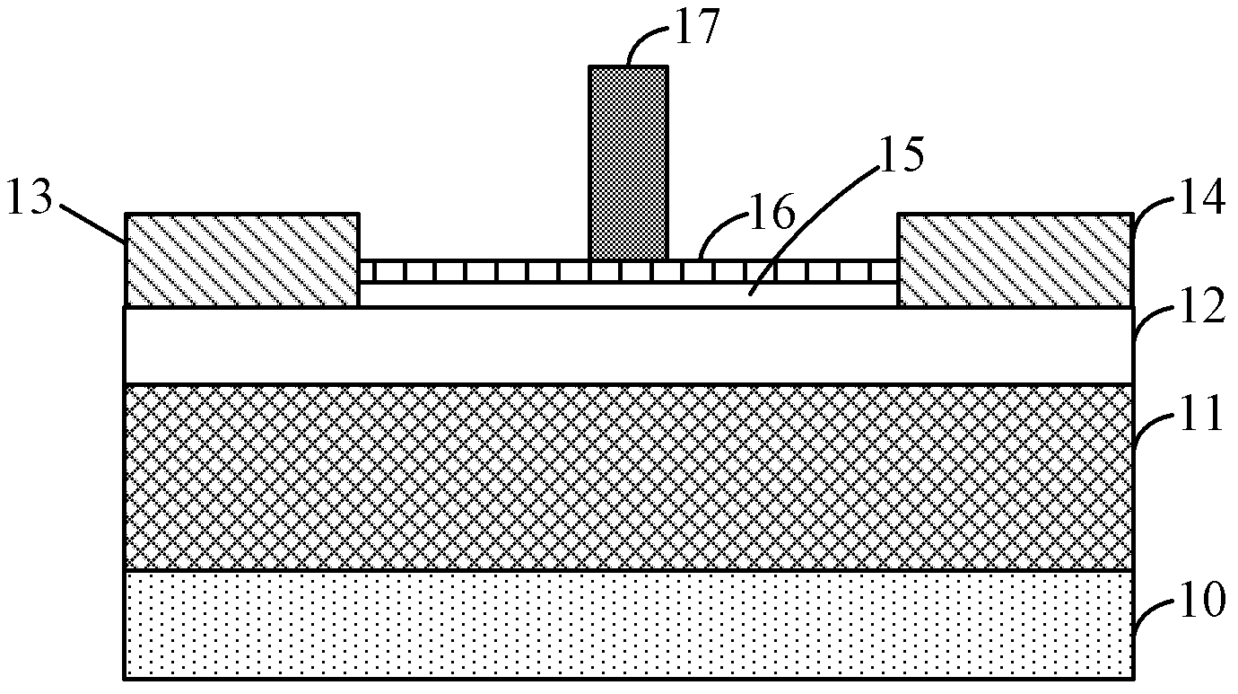
[0040] Example 1: Graphene is used as the conductive channel, metal titanium / gold is used as the source-drain electrode, polyvinylphenol organic dielectric layer and atomic layer deposited hafnium oxide are used as the composite gate dielectric layer, and metal nickel / gold is used as graphite for the gate electrode ene field effect transistor.

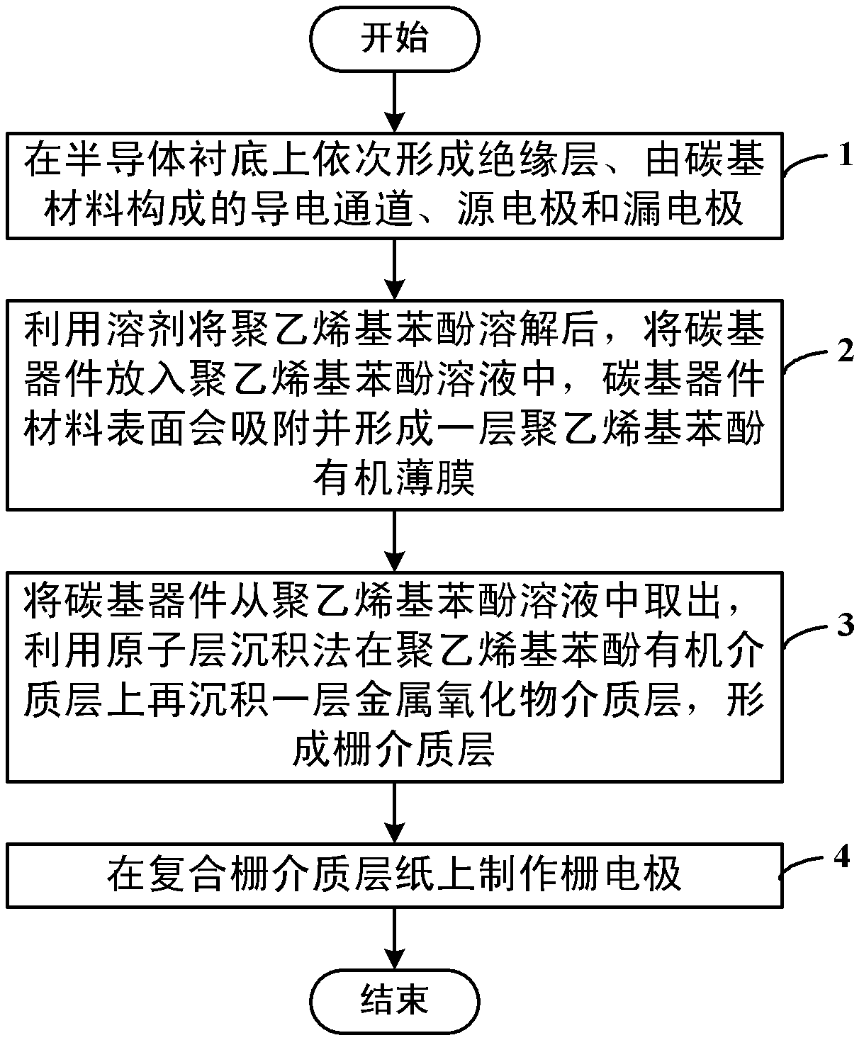
[0041] Concrete preparation steps are as follows:

[0042]Step 1: On the graphene material on the 100nm silicon dioxide / bulk silicon substrate sheet, after forming the source-drain electrode shape by electron beam lithography, electron beam evaporates a layer of 10nm / 50nm thick titanium / gold (Ti / Au= 10 / 50nm) metal as the source-drain electrode, and then put the sample into acetone to peel off, remove the unnecessary metal layer, and obtain the source-drain metal electrode;

[0043] Step 2: Prepare polyvinyl phenol solution, dissolve polyvinyl phenol in propylene glycol methyl ether acetate to form a polyvinyl phenol solution, then soa...

Embodiment 2

[0046] Example 2: Using carbon nanotubes as the conductive channel, using metal titanium / gold as the source and drain electrodes, using polyvinylphenol organic dielectric layer and atomic layer deposition hafnium oxide as the gate composite dielectric layer, and metal nickel / gold as the gate electrode Graphene Field Effect Transistor.

[0047] The specific steps are similar to Example 1, but carbon nanotubes are used as conductive channels.

Embodiment 3

[0048] Embodiment 3: a graphene field effect transistor with metal titanium / gold as the source and drain electrodes, polyvinylphenol organic dielectric layer and atomic layer deposition hafnium oxide as the gate compound dielectric layer, and metal nickel / gold as the gate electrode.

[0049] The specific steps are similar to Example 1, but in Step 2, polyvinylphenol is dissolved in deionized water to form a polyvinylphenol solution.


PUM


Abstract

The invention discloses a carbon-based field effect transistor and a preparing method of the transistor. The carbon-based field effect transistor comprises a semiconductor substrate, an insulating layer formed on the semiconductor substrate, a conductive channel formed on the insulating layer, a source electrode and a drain electrode which are formed at the two ends of the conductive channel respectively, a composite gate dielectric layer formed between the source electrode and the drain electrode and on the conductive channel, and a gate electrode formed on the composite gate dielectric layer. The problem that a gate dielectric film with a high dielectric constant can not directly grow on the conductive channel formed by a carbon-based material by means of atomic layer deposition is solved. Polyvinyl phenol provides a nucleation center for the atomic layer deposition, meanwhile does not cause remarkable decreasing of carrier mobility of the carbon-base material, and does not cause reduction of device performance.

Description

technical field [0001] The invention relates to a field-effect transistor and a preparation method thereof, a carbon-based field-effect transistor and a preparation method thereof, and belongs to the technical field of nanoelectronics. Background technique [0002] Nanoelectronics based on carbon materials, especially those based on carbon nanotubes (Carbon Nanotube) and graphene (Graphene), are considered to have great application prospects and great potential to replace silicon-based materials. Since the successful development of carbon nanotubes in 1991 and graphene in 2004, carbon-based electronics has made great progress. Carbon-based electronics have attracted more and more attention because of their small size, high speed, low power consumption, and simple process. [0003] The performance of field effect transistors is affected by two most important factors, one is the material properties, which determine the potential of device performance; the other is the gate di...

Claims


Application Information

Patent Timeline
Patent Type & Authority Applications(China)
IPC IPC(8): H01L29/78H01L29/51H01L21/336H01L21/285
Inventor 麻芃金智史敬元张大勇彭松昂
Owner INST OF MICROELECTRONICS CHINESE ACAD OF SCI
Why Eureka
Try Eureka