Semiconductor Structures with Rare-earths

a technology of rare earths and semiconductors, applied in the field of solid-state devices, can solve the problems of poor interface quality, degradation of device reliability, and limited practical application of such a schem

a technology of rare earths and semiconductors, applied in the field of solid-state devices, can solve the problems of poor interface quality, degradation of device reliability, and limited practical application of such a schem

US20090236595A1Active Publication Date: 2009-09-24IQE

Image

  • Semiconductor Structures with Rare-earths
  • Semiconductor Structures with Rare-earths
  • Semiconductor Structures with Rare-earths

Examples


Embodiment Construction

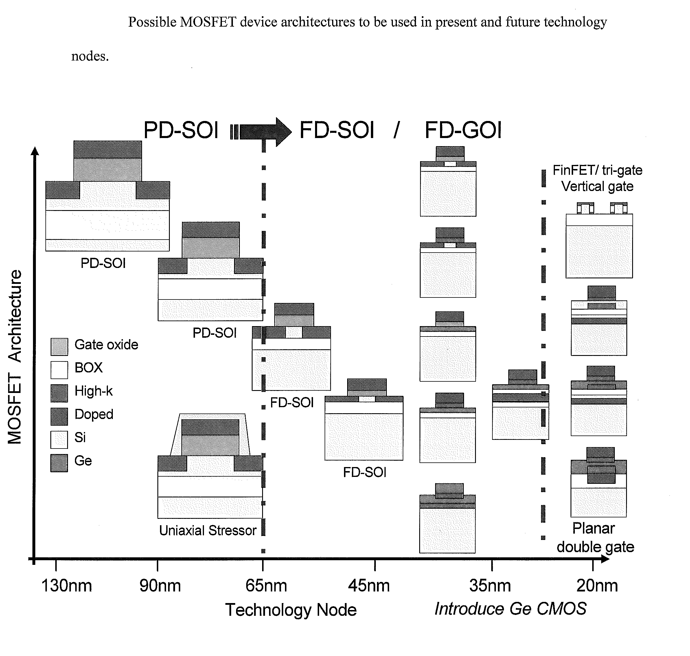
[0063]Epi-Twist Technology

[0064]In some embodiments, Erbium or Ytterbium are used to form a cubic crystalline oxide (c-ErOx), wherein x may range from 0≦x≦5. The electrical properties of ErOx, with a band gap of ˜6 eV, make it a candidate as an insulator and possible high-k gate oxide. The optical refractive index of ErOx is very close to stoichiometric silicon nitride, Si3N4. In some embodiments single process deposition of epitaxial silicon is deposited on cubic-ErOx, with the rare-earth oxide itself deposited on Si (111) or (100) surfaces. The Si epi-layer retains the crystal orientation of the ErOx. The cubic-ErOx layer can be deposited under conditions such that the initial Si surface orientation is transferred to the Si cap—thereby generating an epitaxial SOI structure—epi-SOI. FIG. 9 is one example of an Epi-twist structure. In this example (110) ErOx is deposited on (100) silicon; sequentially (110) silicon is deposited on the (110) ErOx surface. Thus a different surface ori...


PUM

PropertyMeasurementUnit
temperatureaaaaaaaaaa
widthaaaaaaaaaa
widthaaaaaaaaaa

Abstract

The present invention discloses structures to increase carrier mobility using engineered substrate technologies for a solid state device. Structures employing rare-earth compounds enable heteroepitaxy of different semiconductor materials of different orientations.

Description

CROSS REFERENCE TO RELATED APPLICATIONS[0001]Applications and patents Ser. Nos. 09 / 924,392, 10 / 666,897, 10 / 746,957, 10 / 799,549, 10 / 825,912, 10 / 825,974, 11 / 022,078, 11 / 025,363, 11 / 025,680, 11 / 025,681, 11 / 025,692, 11 / 025,693, 11 / 084,486, 11 / 121,737, 11 / 187,213, U.S. 20050166834, U.S. 20050161773, U.S. 20050163692, Ser. Nos. 11 / 053,775, 11 / 053,785, 11 / 054,573, 11 / 054,579, 11 / 054,627, 11 / 068,222, 11 / 188,081, 11 / 253,525, 11 / 254,031, 11 / 257,517, 11 / 257,597, 11 / 393,629, 11 / 398,910, 11 / 472,087, 11 / 788,153, 60 / 533,378, 60 / 811,311, 60 / 820,438, 60 / 847,767, 60 / 876,182, 60 / 905,415, 60 / 944,369, 60 / 949,753, US7,018,484, U.S. 2006 / 0220090, U.S. 2006 / 0065930, U.S. 2006 / 0197124, U.S. Pat. No. 6,734,453, U.S. Pat. No. 7,023,011, U.S. Pat. No. 6,858,864, U.S. Pat. No. 7,037,806, U.S. Pat. No. 7,135,699, and U.S. Pat. No. 7,199,015, all held by the same assignee, contain information relevant to the instant invention and are included herein in their entirety by reference.PRIORITY[0002]This application cl...

Claims


Application Information

Patent Timeline
24 Sep 2009
Publication
US20090236595A1
IPC
H01L29/786
CPC
H01L21/02381; H01L27/1207; H01L21/02433; H01L21/02488; H01L21/02516; H01L21/02532; H01L21/02538; H01L21/02551
Inventors
ATANACKOVIC, PETAR B.