Mos device structure

a technology of mos and device structure, which is applied in the direction of semiconductor devices, electrical equipment, transistors, etc., can solve the problems of limiting the application of transistors and reducing the device performance, and achieve the effect of reducing the damage caused by ion implantation and restricting the boron channeling

Inactive Publication Date: 2009-07-02
UNITED MICROELECTRONICS CORP
View PDF2 Cites 114 Cited by
  • Summary
  • Abstract
  • Description
  • Claims
  • Application Information

AI Technical Summary

Benefits of technology

[0008]The invention provides a method of forming a metal-oxide-semiconductor (MOS) device, which can restrain boron channeling effects and alleviating possible damages caused by ion implantation.

Problems solved by technology

However, due to the limitations in mobility of electrons and holes in silicon, the applications of the transistors are confined.
However, certain issues still exist in the manufacturing processes involving using SEG process, which may downgrade the device performances.

Method used


Image

  • Mos device structure
  • Mos device structure
  • Mos device structure

Examples


Embodiment Construction

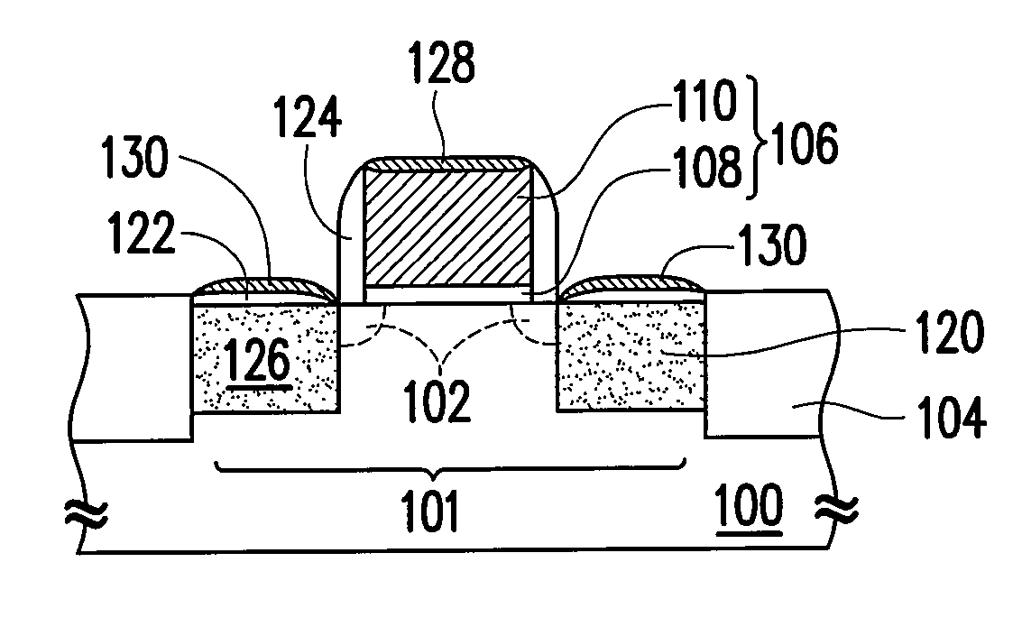
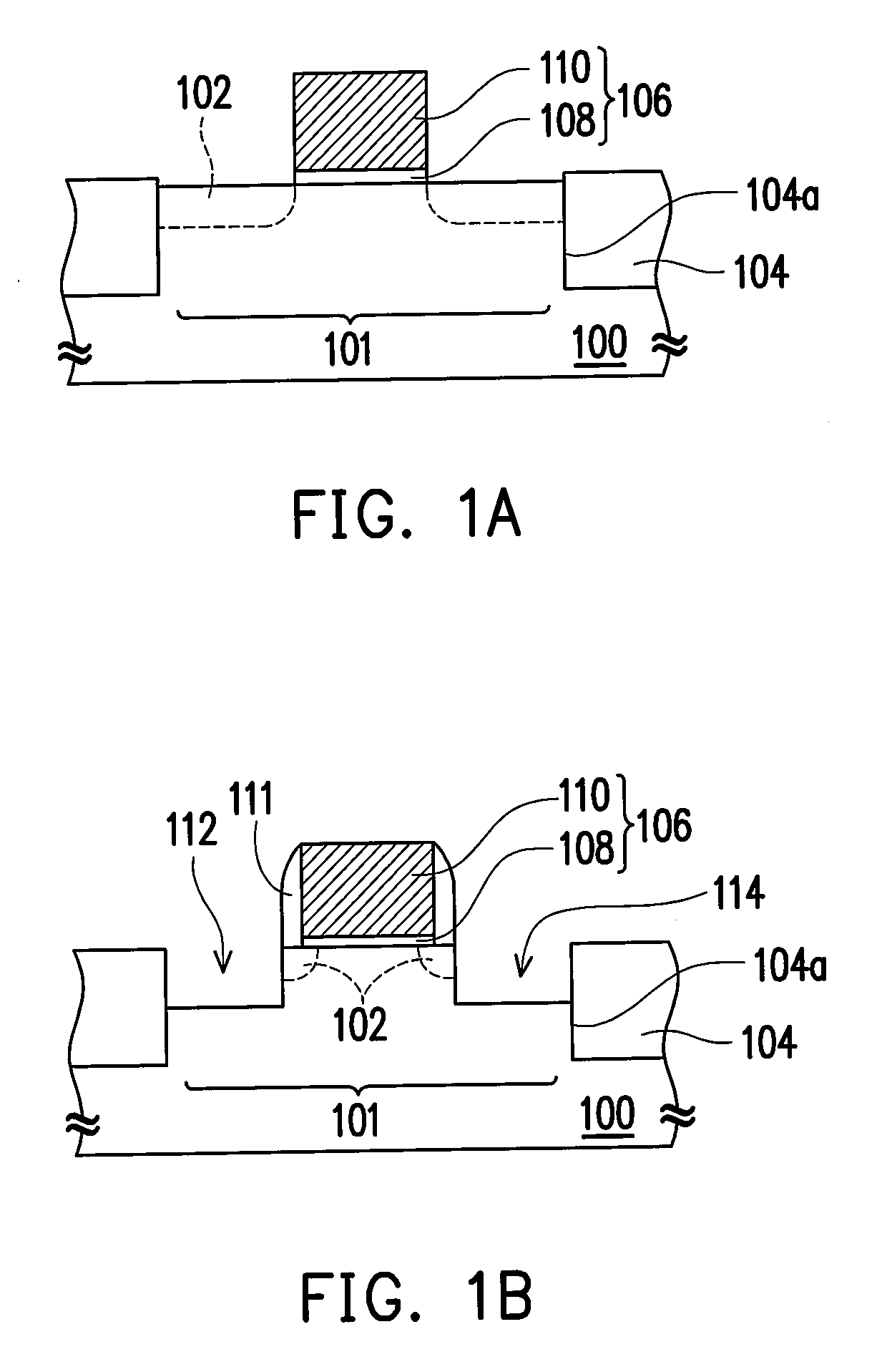
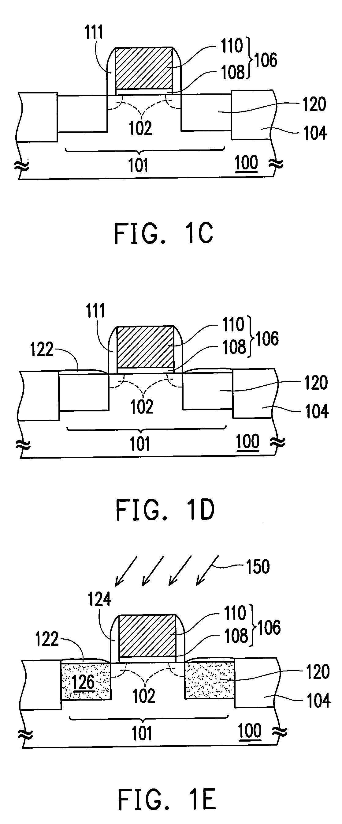
[0024]FIGS. 1A-1F are cross-sectional views of the manufacture processes for forming a semiconductor device structure according to one preferred embodiment of this invention.

[0025]Referring to FIG. 1A, a substrate 100 e.g. a monocrystalline silicon substrate is provided. A trench 104a is formed in the substrate 100, and an isolation structure 104 is formed in the trench 104a so as to define an active region 101. The isolation structure 104 is made of an insulating material e.g. silicon oxide and is formed by performing a chemical vapor deposition process, for example.

[0026]Then, a gate structure 106 is formed on the substrate 100 within the active region 101. The gate structure 106 is composed of a gate dielectric layer 108 and a conductive layer 110. Here, the gate structure 106 is formed by forming a dielectric material layer (not shown) on the substrate 100 within the active region 101. The dielectric material layer is made of silicon oxide, for example. Next, a conductive materi...


PUM


Abstract

The present invention provides a method for forming a metal-oxide-semiconductor (MOS) device and the structure thereof. The method includes at least the steps of forming a silicon germanium layer by the first selective epitaxy growth process and forming a cap layer on the silicon germanium layer by the second selective epitaxy growth process. Hence, the undesirable effects caused by ion implantation can be mitigated.

Description

BACKGROUND OF THE INVENTION[0001]1. Field of Invention[0002]The present invention relates to a semiconductor device and manufacture method thereof. More particularly, the present invention relates to a manufacture method of forming semiconductor device with improved characteristics, and the semiconductor device structure thereof.[0003]2. Description of Related Art[0004]The metal-oxide-semiconductor (MOS) transistor is one of the most important devices widely applied for very-large-scale-integration (VLSI) circuits, including logic circuits, microprocessors and memories. In addition to a gate oxide layer and a conductive gate structure, the MOS transistor further includes a source / drain region having dopants with a conductivity type opposite to that of the substrate.[0005]With the rapid developments of electronic products e.g. telecommunication products, operating speed of transistors is bound to increase. However, due to the limitations in mobility of electrons and holes in silicon,...

Claims


Application Information

Patent Timeline
Patent Type & Authority Applications(United States)
IPC IPC(8): H01L29/04H01L21/336
CPCH01L29/665H01L29/6659H01L29/7848H01L29/7834H01L29/66636
Inventor TING, SHYH-FANNHSU, SHIH-CHIEHHUANG, CHENG-TUNGWU, CHIH-CHIANGHUNG, WEN-HANWU, MENG-YIJENG, LI-SHIANSHIH, CHUNG-MINLEE, KUN-HSIENCHENG, TZYY-MING
Owner UNITED MICROELECTRONICS CORP
Why Eureka
Try Eureka