Finfet with longitudinal stress in a channel

a technology of longitudinal stress and fin, which is applied in the direction of basic electric elements, semiconductor devices, electrical equipment, etc., can solve the problems of difficult formation of embedded stress-generating structures in fins, ineffective lengthwise generation of stress, and difficulty in channel stress introduction to enhance the mobility of charge carriers. , to achieve the effect of enhancing device performan

Active Publication Date: 2010-02-18
GLOBALFOUNDRIES US INC
View PDF17 Cites 120 Cited by
  • Summary
  • Abstract
  • Description
  • Claims
  • Application Information

AI Technical Summary

Benefits of technology

[0007]The present invention provides a fin field effect transistors (finFET) having longitudinal stress, which may be advantageously employed to enhance the device performance, and methods of manufacturing the same.
[0008]According to the present invention, at least one semiconductor fin is formed on an insulator layer. At least one gate dielectric, a gate electrode, and a gate cap dielectric are formed over at least one channel region of the at least one semiconductor fin. A gate spacer is formed on the sidewalls of the gate electrode, exposing end portions of the fin on both sides of the gate electrode. The exposed portions of the semiconductor fin are vertically and laterally etched, thereby reducing the height and width of the at least one semiconductor fin in the end portions. Exposed portions of the insulator layer may also be recessed. A lattice-mismatched semiconductor material is grown on the remaining end portions of the at least one semiconductor fin by selective epitaxy with epitaxial registry with the at least one semiconductor fin. The lattice-mismatched material applies longitudinal stress along the channel of the finFET formed on the at least one semiconductor fin, which is employed to enhance performance of the finFET.

Problems solved by technology

One of the challenges for a finFET is the difficulty of introducing stress into the channel to enhance the mobility of charge carriers.
Formation of an embedded stress-generating structure in a fin is difficult the fin typically protrudes above an insulator surface and does not have lateral support.
Formation of a stress generating liner over a fin generates stress in the widthwise direction of the fin, but is not effective in generating stress in lengthwise direction.

Method used


Image

  • Finfet with longitudinal stress in a channel
  • Finfet with longitudinal stress in a channel
  • Finfet with longitudinal stress in a channel

Examples


Embodiment Construction

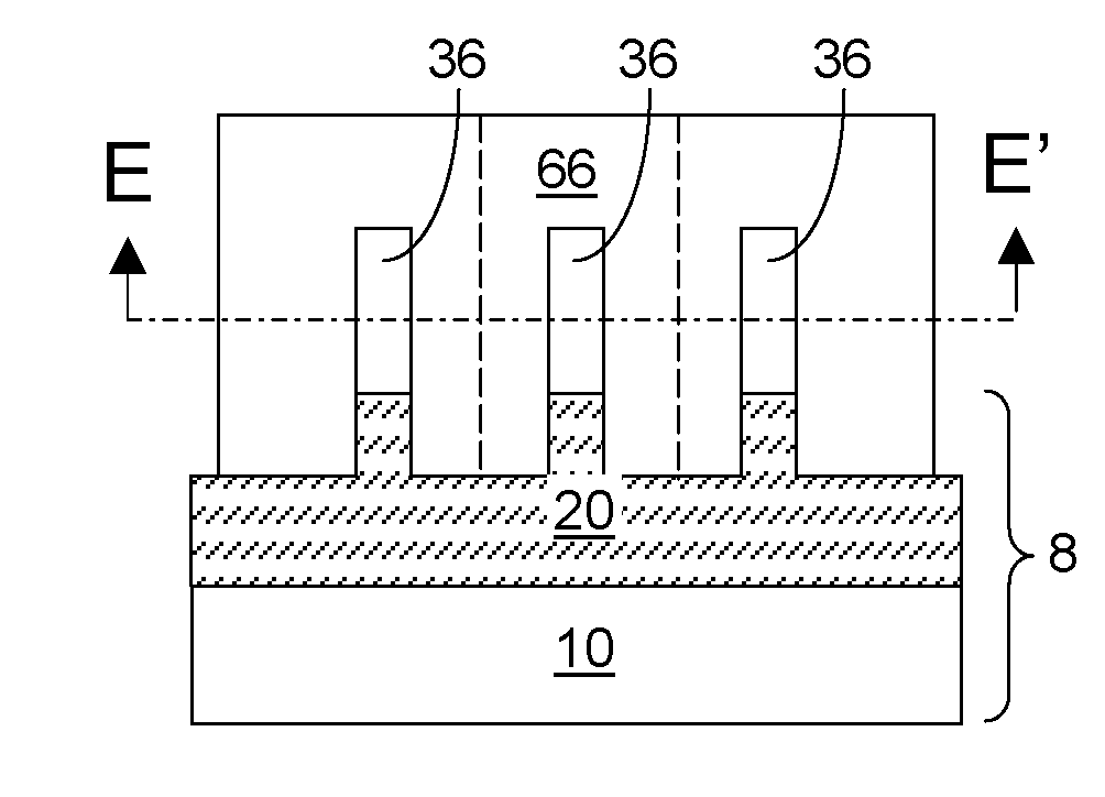
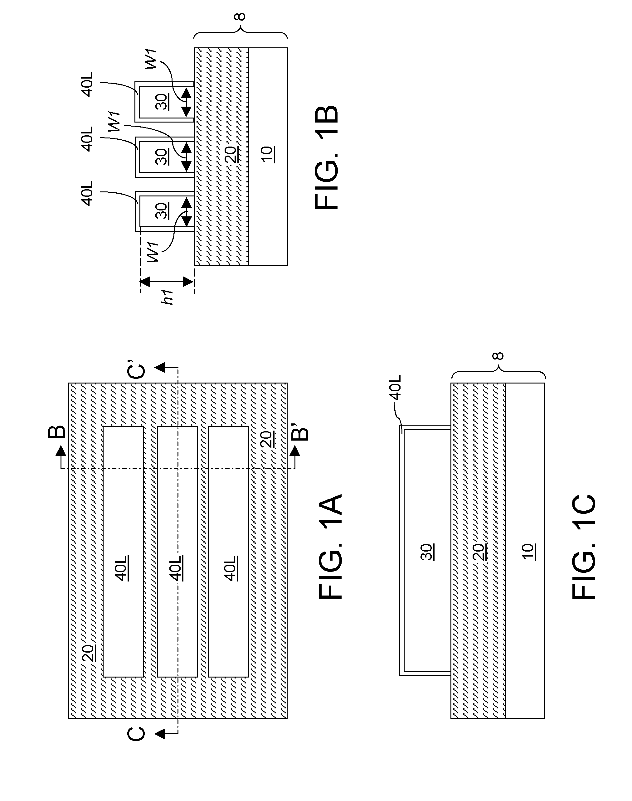
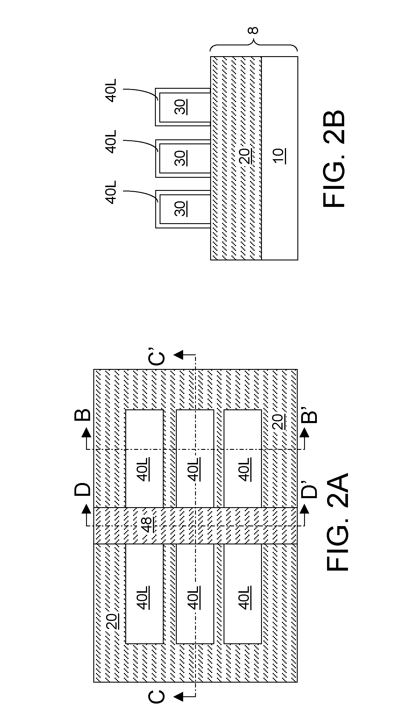
[0029]As stated above, the present invention relates to a fin field effect transistor (finFET) having a longitudinal stress in a channel, and methods of manufacturing the same, which are now described in detail with accompanying figures. As used herein, when introducing elements of the present invention or the preferred embodiments thereof, the articles “a”, “an”, “the” and “said” are intended to mean that there are one or more of the elements. Throughout the drawings, the same reference numerals or letters are used to designate like or equivalent elements. Detailed descriptions of known functions and constructions unnecessarily obscuring the subject matter of the present invention have been omitted for clarity. The drawings are not necessarily drawn to scale.

[0030]Referring to FIGS. 1A-1C, an exemplary semiconductor structure according to the present invention comprises a substrate 8 containing a handle substrate layer 10 and an insulator layer 20. The handle substrate layer 10 may...


PUM


Abstract

At least one gate dielectric, a gate electrode, and a gate cap dielectric are formed over at least one channel region of at least one semiconductor fin. A gate spacer is formed on the sidewalls of the gate electrode, exposing end portions of the fin on both sides of the gate electrode. The exposed portions of the semiconductor fin are vertically and laterally etched, thereby reducing the height and width of the at least one semiconductor fin in the end portions. Exposed portions of the insulator layer may also be recessed. A lattice-mismatched semiconductor material is grown on the remaining end portions of the at least one semiconductor fin by selective epitaxy with epitaxial registry with the at least one semiconductor fin. The lattice-mismatched material applies longitudinal stress along the channel of the finFET formed on the at least one semiconductor fin.

Description

FIELD OF THE INVENTION[0001]The present invention relates to a semiconductor device, and particularly, to a fin field effect transistor (finFET) having a longitudinal stress in a channel, and methods of manufacturing the same.BACKGROUND OF THE INVENTION[0002]A fin metal-oxide-semiconductor field effect transistor (FinMOSFET, or finFET) provides solutions to metal-oxide-semiconductor field effect transistor (MOSFET) scaling problems at, and below, the 45 nm node of semiconductor technology. A finFET comprises at least one narrow (preferably <30 nm wide) semiconductor fin gated on at least two opposing sides of each of the at least one semiconductor fin. Prior art finFET structures are typically formed on a semiconductor-on-insulator (SOI) substrate, because of low source / drain diffusion to substrate capacitance and ease of electrical isolation by shallow trench isolation structures.[0003]A feature of a finFET is a gate electrode located on at least two sides of the channel of the ...

Claims


Application Information

Patent Timeline
Patent Type & Authority Applications(United States)
IPC IPC(8): H01L27/12H01L21/84
CPCH01L29/66795H01L29/785H01L29/7848
Inventor CHAN, KEVIN K.PARK, DAE-GYUWANG, XINHUI
Owner GLOBALFOUNDRIES US INC
Why Eureka
Try Eureka