Operation scheme for programming charge trapping non-volatile memory

a non-volatile memory and operation scheme technology, applied in static storage, digital storage, instruments, etc., can solve the problems of difficult to predict the threshold voltage of the memory cell, time-consuming verification operation, and memory cells in a large array that do not all behave uniformly, so as to reduce or eliminate verification operations, reduce the overall time required for program operation, and improve device performance

Active Publication Date: 2005-12-22
MACRONIX INT CO LTD
View PDF65 Cites 110 Cited by
  • Summary
  • Abstract
  • Description
  • Claims
  • Application Information

AI Technical Summary

Benefits of technology

[0010] The present invention provides a method for self-converging programming of a multiple-bit per cell, charge storage memory cell having a source and a drain in a substrate, a charge storage element and a control gate. In one embodiment, the method includes determining a data value from one of more than two data values to be stored in the memory cell, and applying a gate voltage to the control gate at one of a predetermined set of gate voltage levels selected in response to the determined data value. Programming parameters are controlled to establish a self-converging threshold state that is determined by the selected gate voltage. In this manner, the threshold voltage converges on a target threshold corresponding with the determined data value for the memory cell. Program verify operations are reduced or eliminated in various embodiments, reducing the overall time required for the program operation, and improving device performance.

Problems solved by technology

One basic problem being addressed by these variations arises because the memory cells in a large array do not all behave uniformly during a programming operation.
The wide distribution of charge after a program pulse makes it difficult to predict the threshold voltage of the memory cell.
The verify operation is time-consuming, and requires complex program algorithms and supporting circuitry.

Method used


Image

  • Operation scheme for programming charge trapping non-volatile memory
  • Operation scheme for programming charge trapping non-volatile memory
  • Operation scheme for programming charge trapping non-volatile memory

Examples


Embodiment Construction

[0031] A detailed description of embodiments of the present invention is provided with reference to FIGS. 1-10.

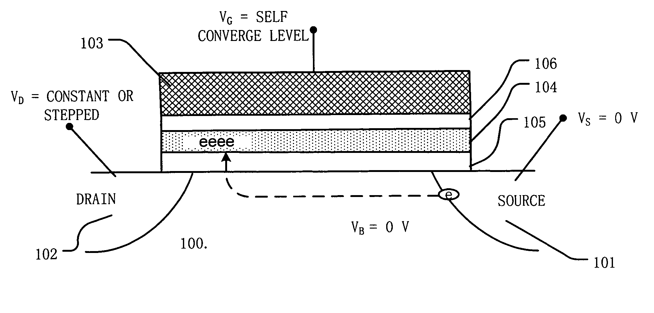
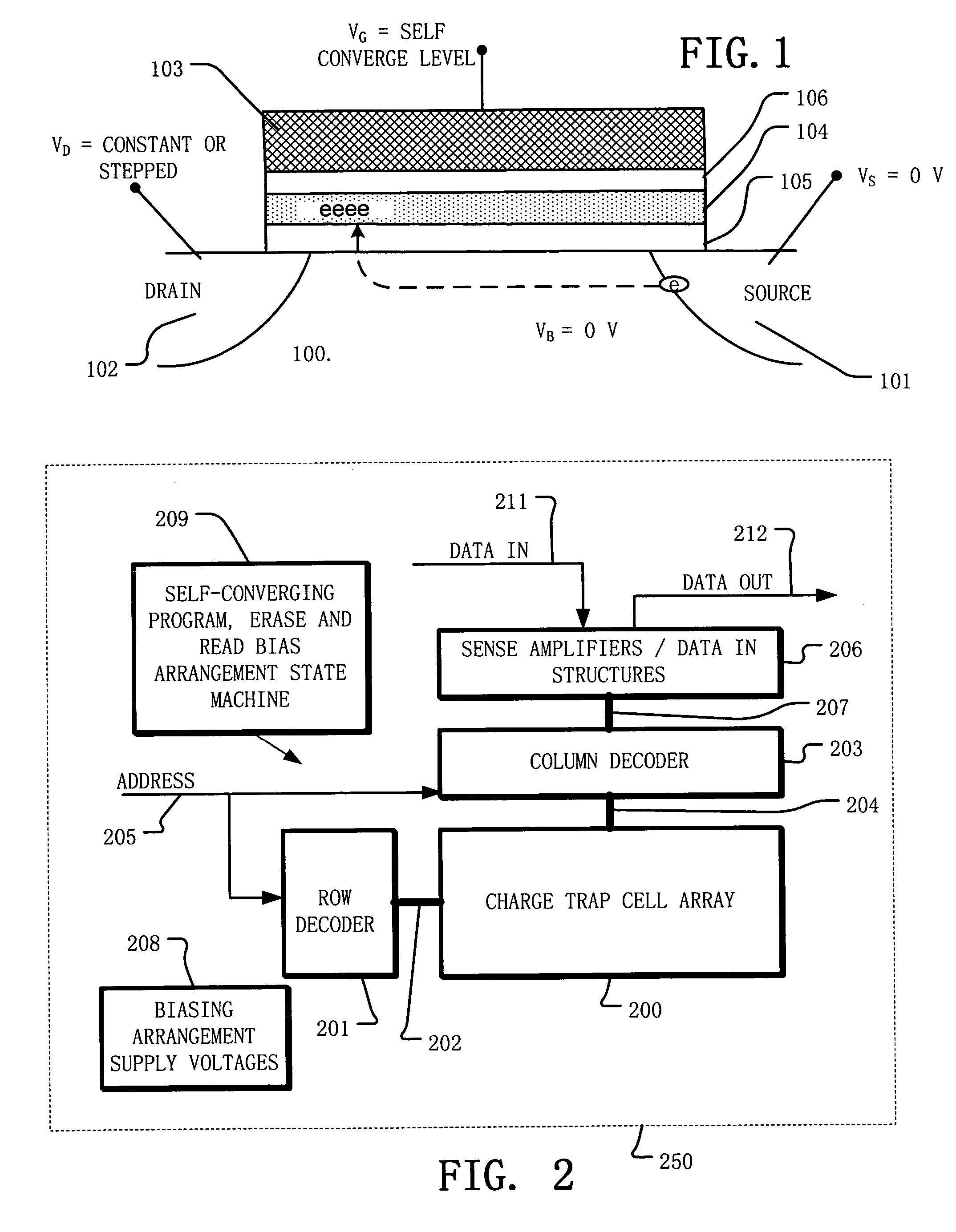
[0032]FIG. 1 is a simplified diagram of an NROM memory cell suitable for use in embodiments of the present invention. The memory cell is implemented in a semiconductor substrate 100. The cell includes a source 101 and a drain 102 formed by respective diffusion regions, separated by a channel in the substrate 100. A control gate 103 overlies the channel. A charge storage element, such as charge trapping layer 104, is isolated by an insulator 106 such as silicon dioxide or silicon oxynitride between the charge trapping layer 104 and the control gate 103 and an insulator, such as gate dielectric 105 comprising silicon dioxide or silicon oxynitride between the charge trapping layer 104 and the channel. The charge trapping layer 104 comprises silicon nitride or silicon oxynitride in typical NROM cells. In other embodiments, other charge trapping material, such as Al2O3, HfOx, Z...


PUM


Abstract

A circuit and method for self-converging programming of a charge storage memory cell, such as NROM or floating gate flash. The method includes determining a data value from one of more than two data values to be stored in the memory cell, and applying a gate voltage to the control gate at one of a predetermined set of gate voltage levels selected in response to the determined data value. Programming parameters are controlled to establish a self-converging threshold state that is determined by the selected gate voltage. In this manner, the threshold voltage converges on a target threshold corresponding with the determined data value for the memory cell. Program verify operations are reduced or eliminated in various embodiments, reducing the overall time required for the program operation, and improving device performance. A second portion of the program operation can include verify operations to improve threshold margins across the array.

Description

RELATED APPLICATIONS [0001] The present application claims the benefit of U.S. Provisional Application No. 60 / 580,518, filed 17 Jun. 2004.BACKGROUND OF THE INVENTION [0002] 1. Field of the Invention [0003] The present invention relates to electrically programmable and erasable non-volatile memory, and more particularly to a programming operation for charge trapping memory. [0004] 2. Description of Related Art [0005] Electrically programmable and erasable non-volatile memory technologies based on charge storage structures known as EEPROM and flash memory are used in a variety of modern applications. A number of memory cell structures are used for EEPROM and flash memory. As the dimensions of integrated circuits shrink, greater interest is arising for memory cell structures based on charge trapping dielectric layers, because of the scalability and simplicity of the manufacturing processes. Memory cell structures based on charge trapping dielectric layers include structures known by th...

Claims


Application Information

Patent Timeline
Patent Type & Authority Applications(United States)
IPC IPC(8): G11C11/34G11C11/56G11C16/04G11C16/10G11C16/34
CPCG11C11/5671G11C16/0466G11C16/3459G11C16/3454G11C16/10
Inventor WU, CHAO-I
Owner MACRONIX INT CO LTD
Why Eureka
Try Eureka