Supercharge Your Innovation With Domain-Expert AI Agents!

A method of manufacturing an array substrate

A manufacturing method and technology for array substrates, which are applied in semiconductor/solid-state device manufacturing, semiconductor devices, electrical components, etc., can solve problems such as insufficient via etching and excessive via etching.

Active Publication Date: 2015-11-25
BOE TECH GRP CO LTD +1
View PDF4 Cites 0 Cited by
  • Summary
  • Abstract
  • Description
  • Claims
  • Application Information

AI Technical Summary

Problems solved by technology

If the process is simplified and a patterning process is applied to the above two via holes, since the depth of the via hole used to connect the source-drain electrode layer and the active layer is different from the depth of the via hole used to connect the shielding layer and the source-drain electrode layer, the required The etching time is also different, so the via hole used to connect the source-drain electrode layer and the active layer is over-etched, and the via hole used to connect the shielding layer and the source-drain electrode layer is not etched in place

Method used


Image

  • A method of manufacturing an array substrate
  • A method of manufacturing an array substrate
  • A method of manufacturing an array substrate

Examples


Embodiment Construction

[0044] The manufacturing method of the array substrate according to the embodiment of the present invention will be described in detail below with reference to the accompanying drawings.

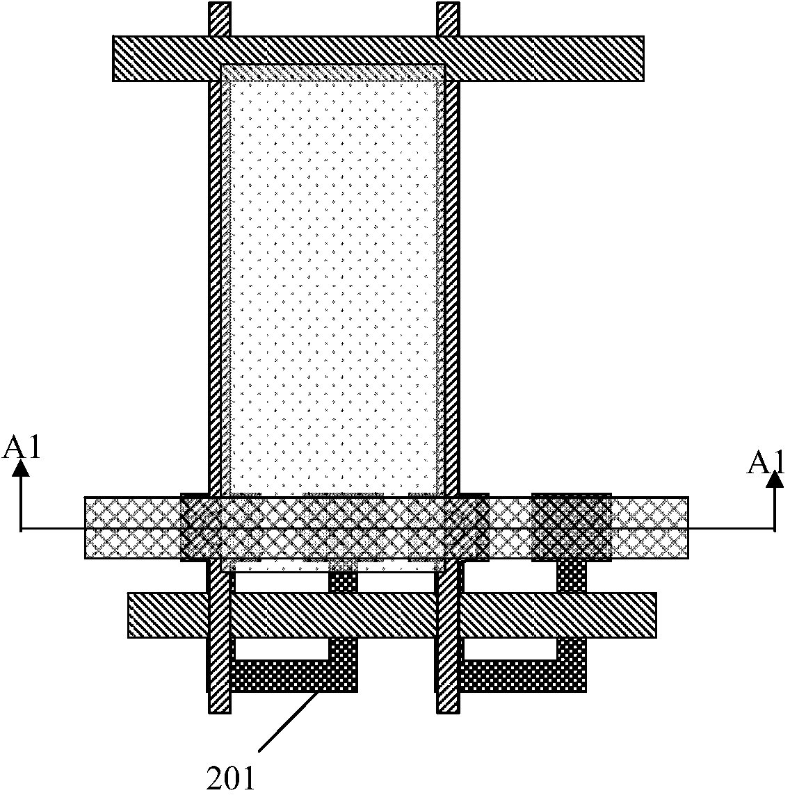
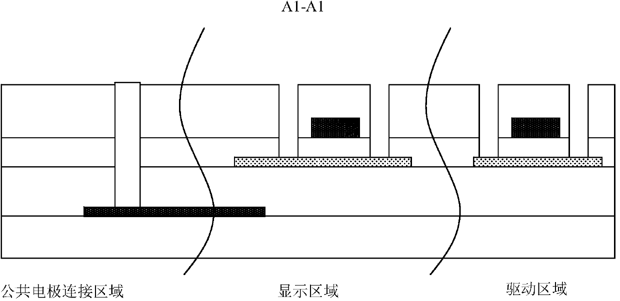
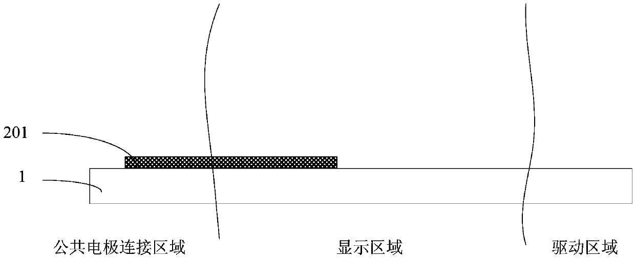
[0045] Such as Figures 2 to 7As shown, the figure shows the cross-sectional structures of three regions, which are respectively the driving region, the display region and the common electrode connection region.

[0046] Such as Figures 2 to 7 As shown, the manufacturing method of the array substrate provided by the embodiment of the present invention includes:

[0047] A shielding layer 201, a buffer insulating layer 301, and an amorphous silicon layer are sequentially formed on a substrate (such as a glass substrate, a quartz substrate, or a plastic substrate, etc.), and the amorphous silicon is crystallized into polysilicon through a polysilicon process. Layer patterns 302, 303, gate insulating layer 401, and NMOS gate 402 in the display area and driving area (the NMOS gate in the driv...


PUM


Abstract

The invention discloses a manufacturing method of an array substrate, which relates to the field of display technology and is designed to simplify the manufacturing process while ensuring the etching quality. The manufacturing method comprises: sequentially forming a shielding layer, a buffer insulating layer, an active Layer, gate insulating layer, NMOS gate in the display area and the drive area; form the PMOS gate in the drive area on the aforementioned substrate, the NMOS gate and the PMOS gate are on the same layer, and are formed in the common electrode connection area at the same time The first via hole is used to connect the shielding layer and the source-drain electrode layer; an intermediate insulating layer is formed on the aforementioned substrate, and the second via hole in the common electrode connection area and the display area and the driving area are formed In the third via hole, the second via hole is in the same position as the first via hole for connecting the shielding layer and the source-drain electrode layer, and the third via hole is used for connecting the active layer and the source-drain electrode layer layer; forming a source-drain electrode layer on the aforementioned substrate. The invention is applicable to the manufacturing process of the array substrate.

Description

technical field [0001] The present invention relates to the field of display technology, in particular to a method for manufacturing an array substrate. Background technique [0002] With the development of low-temperature polysilicon technology, high PPI (PixelPerInch, the number of pixels per inch) products have gradually become the mainstream. The disadvantage of high PPI products is the reduction of storage capacitor area, so additional storage capacitors are required. To compensate for the reduction in the area of ​​the storage capacitor itself, the corresponding countermeasures are mostly to increase the shielding layer at the bottom layer, and the shielding layer is connected to the common electrode, so that the storage capacitance between the shielding layer and the active layer is increased to compensate for the reduction in the storage capacitance itself . [0003] The planar structure of the low-temperature polysilicon array substrate is as follows: Figure 1a As...

Claims


Application Information

Patent Timeline
Patent Type & Authority Patents(China)
IPC IPC(8): H01L21/336H01L21/77H01L27/02
CPCH01L21/76816H01L21/84H01L27/124H01L27/1259H01L21/77H01L27/12H01L21/823871H01L27/1262
Inventor 杨玉清朴承翊李炳天
Owner BOE TECH GRP CO LTD
Features
  • R&D
  • Intellectual Property
  • Life Sciences
  • Materials
  • Tech Scout
  • Unparalleled Data Quality
  • Higher Quality Content
  • 60% Fewer Hallucinations
Learn More