Display substrate and manufacturing method thereof, display panel and display device
A technology of display substrate and manufacturing method, which is applied in semiconductor/solid-state device manufacturing, electrical components, electrical solid-state devices, etc., can solve the problems of complex manufacturing process and increased manufacturing cost of display substrates, etc.
- Summary
- Abstract
- Description
- Claims
- Application Information
AI Technical Summary
Problems solved by technology
Method used
Image

Examples
Embodiment 1
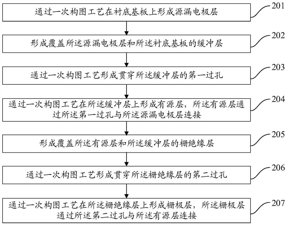
[0060] refer to figure 2 , which shows a flow chart of a method for manufacturing a display substrate according to an embodiment of the present invention, which may specifically include the following steps:
[0061] In step 201, a source-drain electrode layer is formed on the base substrate through a patterning process.
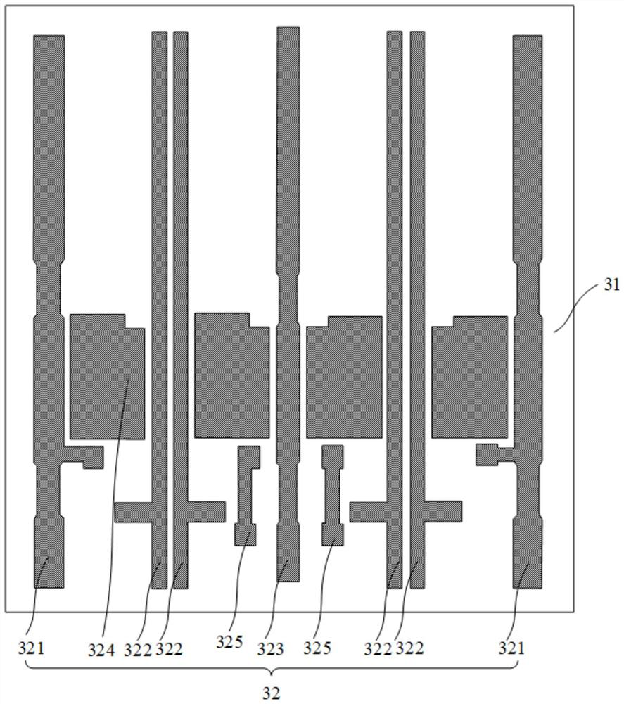
[0062] In the embodiment of the present invention, first, as image 3As shown, a base substrate 31 is provided, and a source-drain electrode layer 32 is formed on the base substrate 31 by a patterning process. Specifically, a source-drain electrode film is first formed on the base substrate 31, a photoresist is coated on the source-drain electrode film, and a mask plate is used to expose the photoresist on the source-drain electrode film. Develop to obtain the photoresist removed area and the photoresist reserved area, etch the source-drain electrode film in the photoresist removed area, and finally peel off the photoresist in the photoresist reserved area...
Embodiment 2
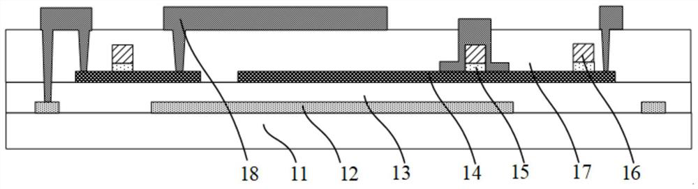
[0128] An embodiment of the present invention provides a display substrate. The display substrate can be manufactured by using the method for manufacturing the display substrate described in the first embodiment above. The display substrate includes: a base substrate 31 ; a source set on the base substrate 31 The drain electrode layer 32; the buffer layer 33 covering the source-drain electrode layer 32 and the base substrate 31; the active layer 34 arranged on the buffer layer 33, the active layer 34 passes through the first via hole of the buffer layer 33 and the source drain The electrode layer 32 is connected; the gate insulating layer 35 arranged on the active layer 34 and the buffer layer 33; the gate layer 36 arranged on the gate insulating layer 35, and the gate layer 36 passes through the second via hole of the gate insulating layer 35 It is connected to the active layer 34 .
[0129] Wherein, the source-drain electrode layer 32 includes a VDD signal line 321, a sensin...
Embodiment 3
[0134] An embodiment of the present invention provides a display panel, including the above-mentioned display substrate.
[0135] In addition, the display panel also includes an encapsulation layer covering the display substrate, and the encapsulation layer may be an organic encapsulation layer, an inorganic encapsulation layer, or a stacked structure of the organic encapsulation layer and the organic encapsulation layer.
[0136] For the specific description of the display substrate, reference may be made to the descriptions of Embodiment 1 and Embodiment 2, which will not be repeated in this embodiment of the present invention.
[0137] An embodiment of the present invention also provides a display device, including the above-mentioned display panel, where the display panel is an OLED display panel.
[0138] In addition, the display device also includes devices such as a driver chip and a TCON (Timer Control Register, timing controller).
[0139] In practical applications, ...
PUM
| Property | Measurement | Unit |
|---|---|---|
| thickness | aaaaa | aaaaa |
| thickness | aaaaa | aaaaa |
| thickness | aaaaa | aaaaa |
Abstract
Description
Claims
Application Information
 - R&D
- Intellectual Property
- Life Sciences
- Materials
- Tech Scout
- Unparalleled Data Quality
- Higher Quality Content
- 60% Fewer Hallucinations
Browse by: Latest US Patents, China's latest patents, Technical Efficacy Thesaurus, Application Domain, Technology Topic, Popular Technical Reports.
© 2025 PatSnap. All rights reserved.Legal|Privacy policy|Modern Slavery Act Transparency Statement|Sitemap|About US| Contact US: help@patsnap.com