CMOS (complementary metal oxide semiconductor) transistor and manufacturing method thereof
A manufacturing method and transistor technology, applied in semiconductor/solid-state device manufacturing, semiconductor devices, electric solid-state devices, etc., can solve the problems of complex low-temperature polysilicon process and high cost of display devices, and achieve the effect of saving manufacturing cost and reducing patterning process
- Summary
- Abstract
- Description
- Claims
- Application Information
AI Technical Summary
Problems solved by technology
Method used
Image

Examples
Embodiment 1
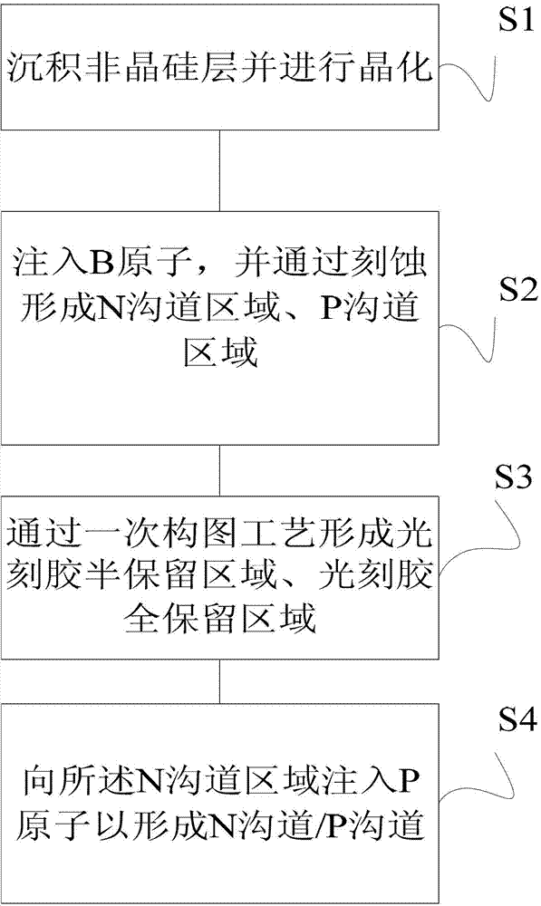
[0044] Such as figure 1 As shown, the present invention provides a method for manufacturing a CMOS transistor, including forming a channel, a gate electrode, an ohmic contact layer, and source and drain electrodes on a substrate; wherein the step of forming the channel includes:
[0045] S1. deposit an amorphous silicon layer on the substrate 1 (such as a transparent glass substrate or a quartz substrate), the preferred thickness of the amorphous silicon layer is Then crystallize the amorphous silicon layer into a polysilicon layer. The crystallization process may include taking a hydrogen removal process for the amorphous silicon, and crystallizing the amorphous silicon to form polysilicon 3 through processes such as laser irradiation;
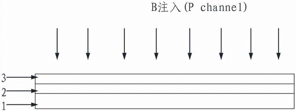
[0046] S2. Implanting boron atoms into the polysilicon layer, the gas used for ion implantation can be B 2 h 6 / H 2 or BF 3 / H 2 ,Such as image 3 shown; then form an N channel region and a P channel region by etching the polysilicon l...
Embodiment 2
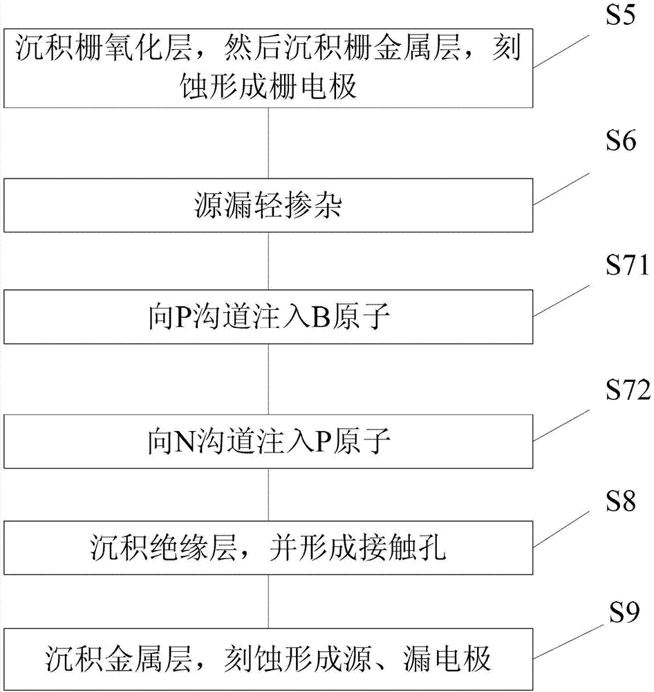
[0062] The present invention also provides a method for manufacturing an array substrate, which includes the aforementioned method for manufacturing a CMOS transistor, and the method for manufacturing an array substrate further includes:
[0063] S10. deposit passivation layer 13 by PECVD method, thickness is preferably And at least two via holes are formed in the passivation layer, and the via holes respectively lead to the drain electrodes of the CMOS transistors;
[0064] S11. Deposit a layer of transparent conductive layer by sputtering or thermal evaporation on the passivation layer made with via holes. The transparent conductive layer is generally ITO or IZO, or other metals and metal oxides, with a thickness of about And form the transparent pixel electrode 14 by photolithography once, there are two transparent pixel electrodes 14, respectively located in the P channel area and the N channel area, and its cross-sectional views are respectively as follows Figure 10 s...
Embodiment 3
[0066] The present invention also provides a CMOS transistor, including a substrate and a channel formed on the substrate, a gate electrode, an ohmic contact layer, and source and drain electrodes; wherein the channel includes an N channel formed in a polysilicon layer implanted with boron atoms A channel area and a P channel area, a photoresist semi-reserved area is set on the N channel area, a photoresist full-reserved area is set on the P channel area, and the photoresist in the photoresist half-reserved area is Removing completely and partially removing the photoresist in the photoresist semi-retained region, implanting phosphorus atoms into the N channel region to form N channel and P channel in the polysilicon layer.
[0067] Optionally, a gate oxide layer and a metal layer having multiple layers of different metals or alloys are sequentially arranged on the P channel, and the metal layer is etched to form a gate electrode.
[0068] Optionally, N-type light doping is per...
PUM
 Abstract
Description
Claims
Application Information
 - R&D
- Intellectual Property
- Life Sciences
- Materials
- Tech Scout
- Unparalleled Data Quality
- Higher Quality Content
- 60% Fewer Hallucinations
Browse by: Latest US Patents, China's latest patents, Technical Efficacy Thesaurus, Application Domain, Technology Topic, Popular Technical Reports.
© 2025 PatSnap. All rights reserved.Legal|Privacy policy|Modern Slavery Act Transparency Statement|Sitemap|About US| Contact US: help@patsnap.com