Active matrix organic light emitting diode backplane and manufacturing method thereof
A light-emitting diode and active matrix technology, which is applied in the field of active matrix organic light-emitting diode backplane and its manufacturing, can solve the problems of preparation oxidation and complex preparation methods, etc.
- Summary
- Abstract
- Description
- Claims
- Application Information
AI Technical Summary
Problems solved by technology
Method used
Image

Examples
preparation example Construction
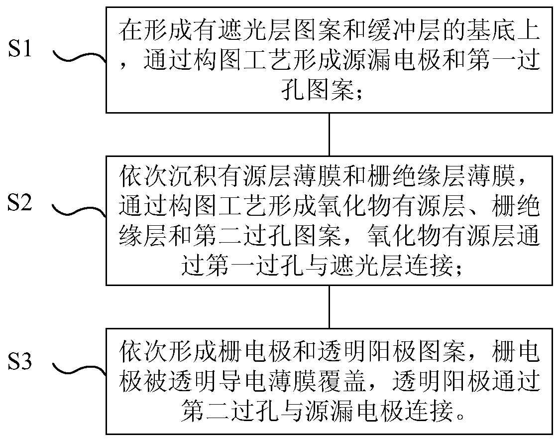
[0063] Such as figure 1 The preparation method of the top gate oxide type AMOLED backplane includes: forming a light-shielding layer pattern on the substrate through the first patterning process; forming a buffer layer and an oxide active layer pattern through the second patterning process; The patterning process forms the gate insulating layer and the gate electrode pattern; the interlayer dielectric layer and the via holes on it are formed through the fourth patterning process; the source and drain electrode patterns are formed through the fifth patterning process, and the source and drain electrodes pass through the interlayer dielectric layer. The opened via holes are connected to the oxide active layer and the light-shielding layer; the color photoresist layer pattern is formed through the sixth patterning process; the planarization layer and the via holes on it are formed through the seventh patterning process; through the eighth patterning process The process forms a tr...
no. 1 example
[0092] Figure 3-10 It is a schematic diagram of preparing an AMOLED backplane according to the first embodiment of the present invention. The AMOLED backplane of this embodiment is based on the COA low-reflection color display solution. The following will combine Figure 3-10 The preparation method of the AMOLED backplane in this embodiment is described in detail. The "patterning process" mentioned in this embodiment includes depositing a film layer, coating photoresist, mask exposure, developing, etching, and stripping photoresist And other treatment, is the existing mature preparation technology. Deposition can use known processes such as sputtering, evaporation, and chemical vapor deposition, coating can use known coating processes, and etching can use known methods, which are not specifically limited here.
[0093] In the first patterning process, a light-shielding layer pattern is formed on the substrate through a single-tone mask patterning process. Forming the ligh...
no. 2 example
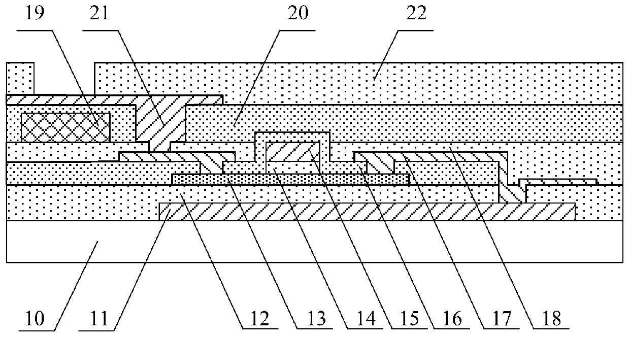
[0117] Based on the inventive concept of the first embodiment, this embodiment provides an AMOLED backplane, which is a top gate type oxide thin film transistor with a non-coplanar structure. The upper and lower sides of the source layer. Such as Figure 10 As shown, the top gate oxide AMOLED backplane in this embodiment includes:
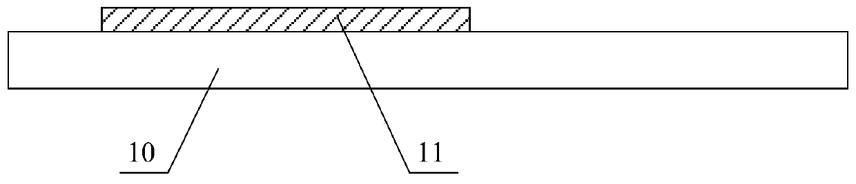
[0118] base 10;
[0119] A light-shielding layer 11 disposed on the substrate 10;
[0120] A buffer layer 12 covering the light-shielding layer 11;
[0121] A source-drain electrode 17 disposed on the buffer layer 12;
[0122] An oxide active layer 13 covering the source and drain electrodes 17, the active layer 13 is connected to the light shielding layer 11 through a first via hole;
[0123] The gate insulating layer 14, gate electrode 15, color photoresist layer 19 and flat layer 20 arranged on the oxide active layer 13; 20 located in the light-emitting area of the sub-pixel;
[0124]A transparent anode 21 arranged in the light-emitting...
PUM
 Abstract
Description
Claims
Application Information
 - R&D
- Intellectual Property
- Life Sciences
- Materials
- Tech Scout
- Unparalleled Data Quality
- Higher Quality Content
- 60% Fewer Hallucinations
Browse by: Latest US Patents, China's latest patents, Technical Efficacy Thesaurus, Application Domain, Technology Topic, Popular Technical Reports.
© 2025 PatSnap. All rights reserved.Legal|Privacy policy|Modern Slavery Act Transparency Statement|Sitemap|About US| Contact US: help@patsnap.com