Wire-bonding method for chips with copper interconnects by introducing a thin layer

Inactive Publication Date: 2005-11-08
NATIONAL CHUNG CHENG UNIV
View PDF3 Cites 116 Cited by
  • Summary
  • Abstract
  • Description
  • Claims
  • Application Information

AI Technical Summary

Benefits of technology

[0008]The primary object of the present invention is to provide a wire-bonding method for chips with copper intercon

Problems solved by technology

On the other hand, the performance of deep sub-micron integrated circuit cannot be further improved since the delay of signal in the interconnect would exceed the delay of signal in the device.
However, one of the disadvantages of copper is that copper is readily oxidized at low temperature, and unlik

Method used


Image

  • Wire-bonding method for chips with copper interconnects by introducing a thin layer
  • Wire-bonding method for chips with copper interconnects by introducing a thin layer
  • Wire-bonding method for chips with copper interconnects by introducing a thin layer

Examples


Embodiment Construction

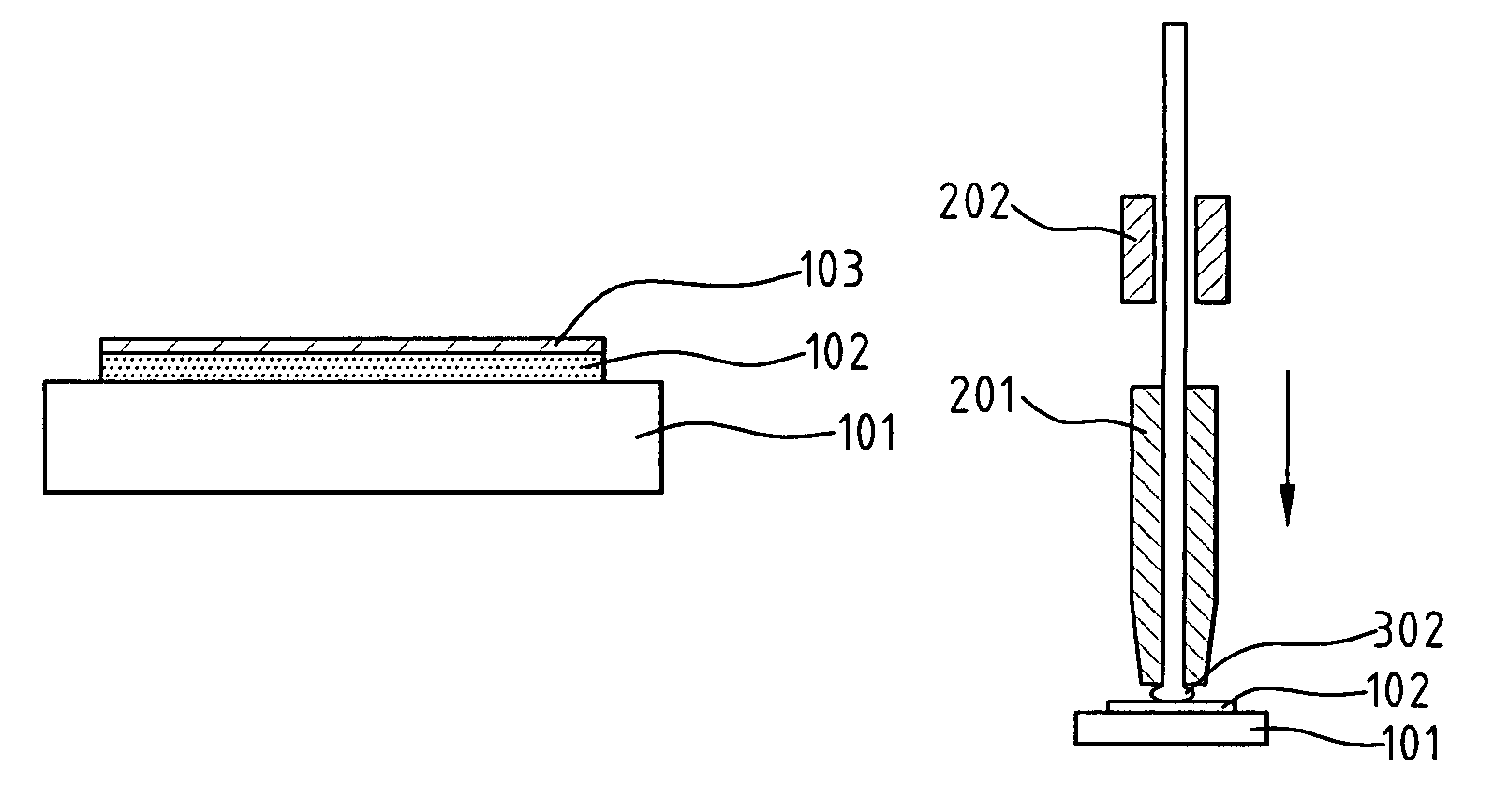
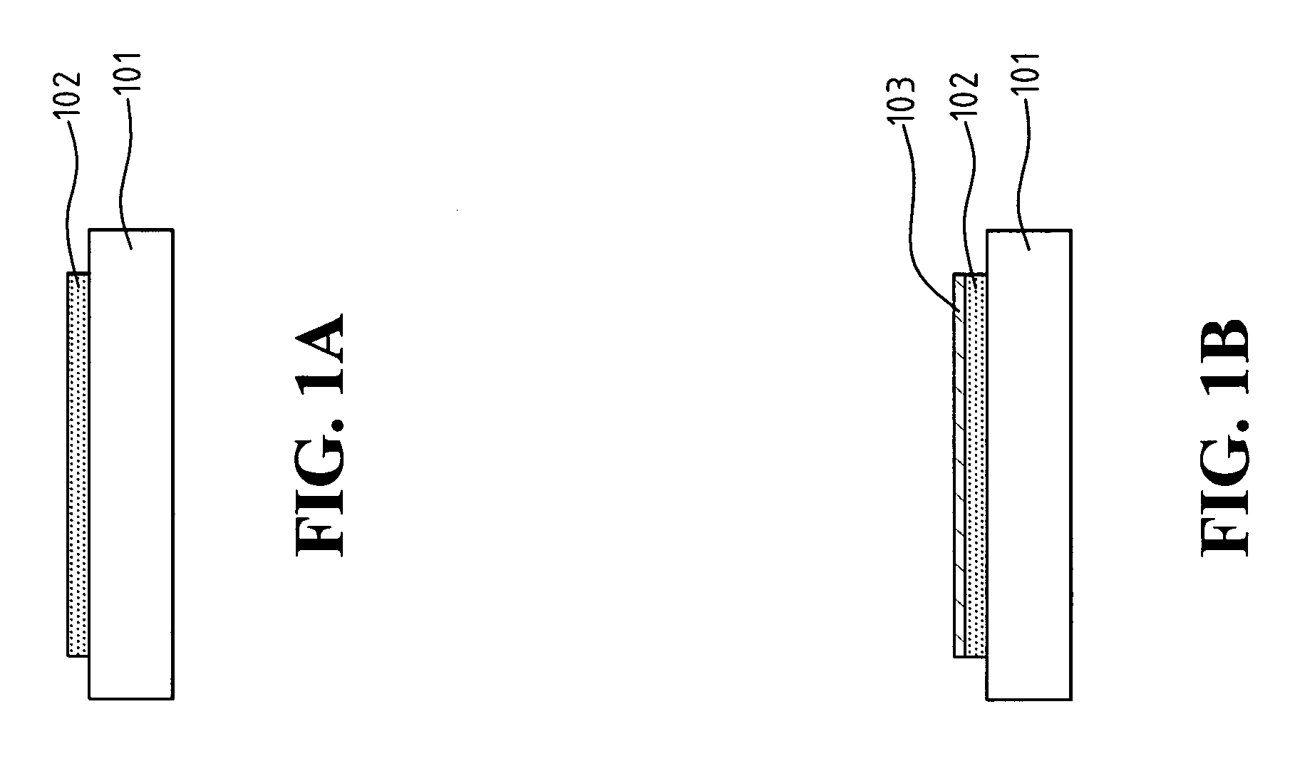
[0016]As shown in FIG. 1A, a chip 101 is provided thereon with a copper bonding-pad 102. The chemical reaction of copper in an aqueous solution is known as: Cu⁢->←⁢Cu++e-(1)Cu⁢->←⁢Cu2++2⁢e-(2)2⁢Cu++H2⁢O⁢->←⁢Cu2⁢O+2⁢H+(3)

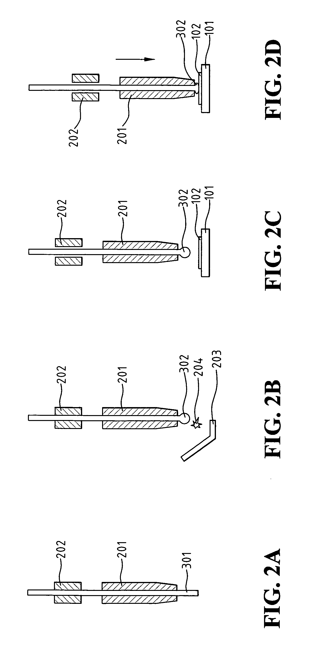
[0017]According to the principle of Le Chatelier, a system would always react in such a way as to tend to counteract the original alteration when the system is in equilibrium and one of the factors, which determine the equilibrium point, is altered. It is understood from reaction (3) that H+is supposed to move to the left side when its concentration is raised up. If the concentration of H+goes up, the aqueous solution is becoming acidified and the pH value is lowered (the higher the H+, the lower the pH value), or vice versa. Therefore, it is possible to keep the reaction going toward the right hand to produce Cuprous oxide (Cu2O) should the concentration of H+is controlled properly under a predetermined level. A preferred concentration of H+below 10−5 M / L, or a pH v...


PUM


Abstract

A wire-bonding method for chips with copper interconnects by introducing a thin layer is provided for solving the problem of oxidizing a copper bonding-pad during bonding processing in order not to deteriorate the bonding strength and yield rate thereof. The wire-bonding method of the present invention comprises: a step for providing a chip with a copper bonding-pad; another step for providing an aqueous solution to form a Cuprous oxide thin layer on the copper bonding-pad; and yet another step for setting a plurality of copper interconnects on the copper bonding-pad and providing an ultrasonic power for removing the Cuprous oxide layer to have the interconnects bonded on the copper bonding-pad.

Description

BACKGROUND OF THE INVENTION[0001]1. Field of the Invention[0002]The present invention relates to the application field regarding IC packaging, particularly to a wire-bonding method for chips with copper interconnects by introducing a thin layer.[0003]2. The Prior Arts[0004]In the VLSI (Very Large Scale Integration) era today, an IC chip is made through several steps including wafer fabricating process, wafer test, VLSI forming process, and finally, IC packaging test.[0005]The packaging test usually comprises a wafer attachment process, a wire-bonding process, etc., in which the wire-bonding process is conducted by a wire bonder for connecting a chip to a plurality of pins with metallic interconnects under a high-temperature and ultrasonic environment. The bonded interconnects serve as a bridge for transmitting signal and / or electric power between a chip and the external circuits. Since, almost all the makers have made different efforts to try minimizing the volume of chip as smaller...

Claims


Application Information

Patent Timeline
IPC IPC(8): H01L21/02H01L21/44H01L21/607H01L23/485
CPCH01L24/03H01L24/05H01L24/48H01L24/85H01L24/45H01L24/78H01L2224/04042H01L2224/05647H01L2224/45144H01L2224/48091H01L2224/48227H01L2224/48247H01L2224/48465H01L2224/78301H01L2224/85045H01L2224/85048H01L2224/85181H01L2224/85205H01L2224/85375H01L2924/01005H01L2924/01006H01L2924/01013H01L2924/01018H01L2924/01022H01L2924/01029H01L2924/01079H01L2924/01082H01L2924/14H01L2924/30105H01L2924/00014H01L2924/01033H01L2924/00H01L2224/48647
Inventor JENG, YEAU-RENCHIU, SANG-MAO
Owner NATIONAL CHUNG CHENG UNIV
Why Eureka
Try Eureka