

Electronic device and manufacturing method thereof
- Summary
- Abstract
- Description
- Claims
- Application Information
AI Technical Summary
Benefits of technology
Problems solved by technology
Method used
Image

Examples
experiment 1
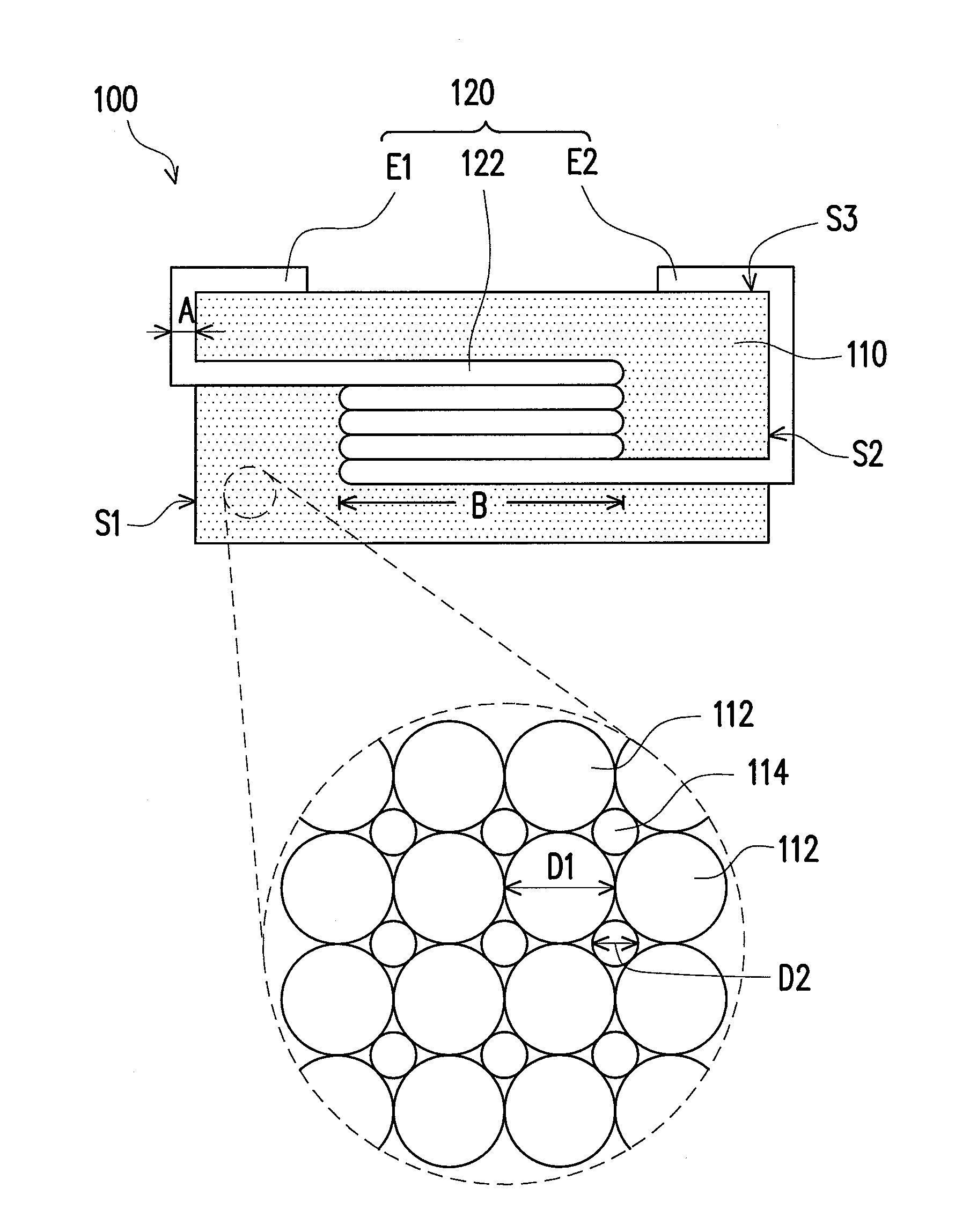
[0059]The structure of an electronic device in Experiment 1 is the same with the structure of the electronic device 100 in FIG. 1. The thread diameter A of the wire 120 is 0.32 mm, the diameter B of the coil is 2.4 mm, the number of turns of the coil is 11.5, and the molding pressure for the magnetic body 110 is 11 t / cm2. The major ingredient, mean particle diameter, and hardness of a first magnetic powder and a second magnetic powder in Experiment 1 are all listed in Table 1.
TABLE 1Mean particlediameterHardnessMajor ingredient(D50)(Hv)First magnetic powderFe—Cr—Si10 μm250Second magneticiron 4 μm30-80powder
[0060]Based on Table 1, the ratio of D1 to D2 is 2.5. FIG. 7 illustrates variation condition of inductance values of the electronic device in two frequencies (25 KHz and 100 KHz) when the ratio of the first magnetic powder to the second magnetic powder in the magnetic body changes. Referring to FIG. 7, the inductance values of an electronic device with the proportion of 20 wt %-80...
experiment 2
[0061]The structure of an electronic device in Experiment 2 is the same with the structure of the electronic device 100 in FIG. 1. The thread diameter A of the wire 120 is 0.32 mm, the diameter B of the coil is 2.4 mm, the number of turns of the coil is 11.5, and the molding pressure for the magnetic body 110 is 11 t / cm2. The major ingredient, mean particle diameter, and hardness of a first magnetic powder and a second magnetic powder in Experiment 2 are all listed in Table 2.
TABLE 2Mean particlediameterHardnessMajor ingredient(D50)(Hv)First magnetic powderAmorphous alloy40 μm900~1,000Second magneticiron 4 μm30~80 powderSecond magneticFe—Cr—Si10 μm250powder
[0062]FIG. 8 illustrates variation condition of inductance values of the electronic device in two frequencies when the ratio of the first magnetic powder to the second magnetic powder in the magnetic body changes. Referring to FIG. 8, the inductance values of the electronic device with the proportion of 20 wt %-80 wt % of the fir...
experiment 3
[0069]The structure of an electronic device in Experiment 3 is the same with the structure of the electronic device 100 in FIG. 1. The thread diameter A of the wire 120 is 0.32 mm, the diameter B of the coil is 2.4 mm, the number of turns of the coil is 13.5, and the molding pressure for the magnetic body 110 is 11 t / cm2. The major ingredient, mean particle diameter, and hardness of a first magnetic powder and a second magnetic powder in Experiment 3 are all listed in Table 5.
TABLE 5Mean particlediameterHardnessMajor ingredient(D50)(Hv)First magnetic powderAmorphous alloy20 μm900~1,000Second magneticiron 4 μm30~80 powder
[0070]Based on Table 5, the ratio of D1 to D2 is 5. FIG. 10A illustrates variation condition of density of a magnetic body and inductance values of an electronic device when the ratio of a first magnetic powder to a second magnetic powder in the magnetic body changes. FIG. 10B illustrates variation condition of density of the magnetic body and permeability of an ele...
PUM
| Property | Measurement | Unit |
|---|---|---|
| Mass | aaaaa | aaaaa |
| Particle diameter | aaaaa | aaaaa |
| Particle diameter | aaaaa | aaaaa |
Abstract
Description
Claims
Application Information