A kind of cmos transistor and its manufacturing method
A manufacturing method and technology for transistors, which are applied in the fields of transistors, semiconductor/solid-state device manufacturing, electrical components, etc., can solve the problems of complex low-temperature polysilicon process and high cost of display devices, and achieve the effect of saving manufacturing costs and reducing patterning processes.
- Summary
- Abstract
- Description
- Claims
- Application Information
AI Technical Summary
Problems solved by technology
Method used
Image

Examples
Embodiment 1
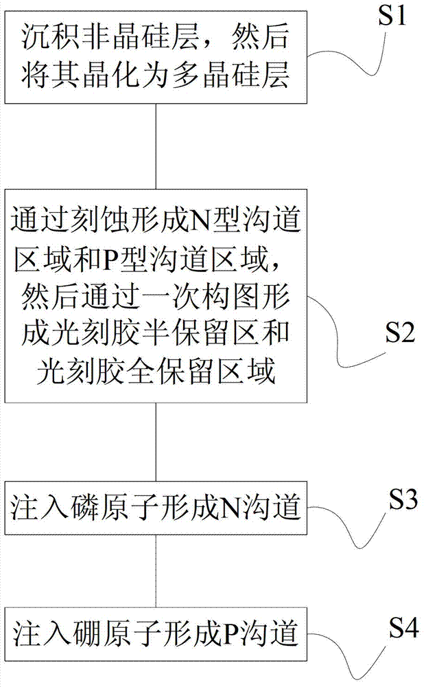
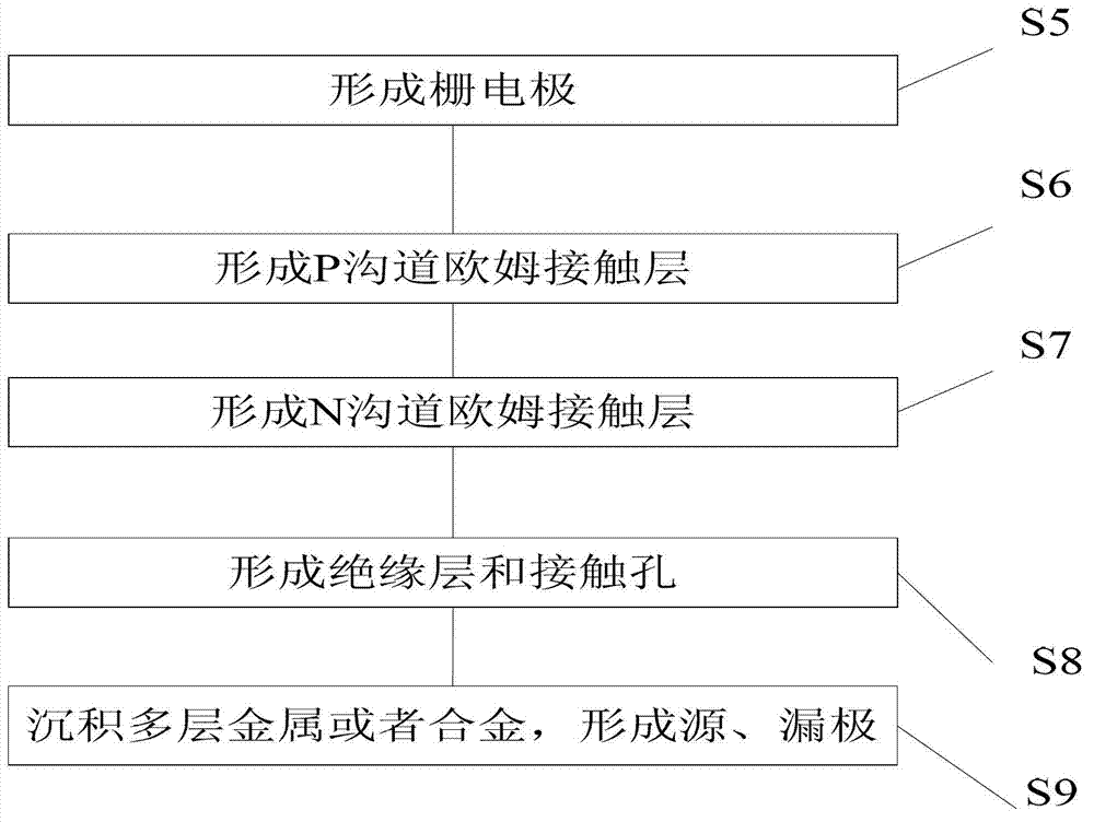
[0044] Such as figure 1 As shown, this embodiment provides a method for manufacturing a CMOS transistor, including forming a channel, a gate electrode, an ohmic contact layer, and source and drain electrodes on a substrate; wherein the step of forming the channel includes:
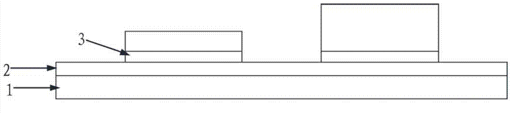
[0045] S1. The thickness deposited on the substrate 1 is The amorphous silicon layer 3, and then take a dehydrogenation process for the amorphous silicon, and crystallize the amorphous silicon layer to form a polysilicon layer 3 through processes such as laser irradiation, and the substrate can be a substrate such as transparent glass or quartz;
[0046] S2. If image 3 As shown, the polysilicon layer is etched to form an N channel region and a P channel region; a photoresist semi-retained region is formed corresponding to the N channel region through a patterning process, and a photoresist semi-retained region is formed corresponding to the P channel region. The track area forms a photoresist fully res...
Embodiment 2
[0062] This embodiment provides a method for manufacturing a low-temperature polysilicon CMOS (complementary metal oxide semiconductor) device array substrate and a TFT-LCD (thin film field-effect transistor LCD) array substrate, which includes the method for manufacturing a CMOS transistor described in Embodiment 1 ,Also includes:
[0063] S10. Deposit thickness by PECVD method is about passivation layer 12, and forming via holes in the passivation layer;
[0064] S11. Deposit a layer thickness of about The transparent conductive layer 13, the transparent conductive layer is generally ITO or IZO, and can also be other metals and metal oxides; the transparent pixel electrode is formed by one photolithography, and its cross-sectional view is as follows Figure 10 shown.
Embodiment 3
[0066] This embodiment also provides a CMOS transistor produced by the above manufacturing method, including a substrate and a channel formed on the substrate, a gate electrode, an ohmic contact layer, and source and drain electrodes; wherein the channel is included in the polysilicon layer Form the N channel region, the photoresist semi-retained region corresponding to the N channel region, the photoresist full reserve region corresponding to the P channel region and the P channel region by one patterning; Removing the photoresist and partially removing the photoresist in the photoresist fully reserved area, implanting phosphorus atoms into the N channel area to form an N channel; Boron atoms are implanted into the channel region to form a P channel.
[0067] The manufacturing process of the CMOS transistor described in this embodiment is simple and stable in performance, and more complex array substrates can be fabricated on this basis.
[0068] Optionally, a gate oxide lay...
PUM
 Abstract
Description
Claims
Application Information