Voltage stabilizing circuit and voltage stabilizing device

一种稳压电路、电流的技术,应用在集成电路领域,能够解决电路功耗大、电荷泵10升高、大功耗等问题,达到降低功耗、克服输出电压不稳定的效果

CN103514951AActive Publication Date: 2014-01-15SEMICON MFG INT (SHANGHAI) CORP
5 Cites 6 Cited by

Patent Information

Authority / Receiving Office
CN · China
Patent Type
Applications(China)
Current Assignee / Owner
Publication Date
2014-01-15

Smart Images

  • Figure 1
    Figure 1
  • Figure 2
    Figure 2
  • Figure 3
    Figure 3
Patent Text Reader

Abstract

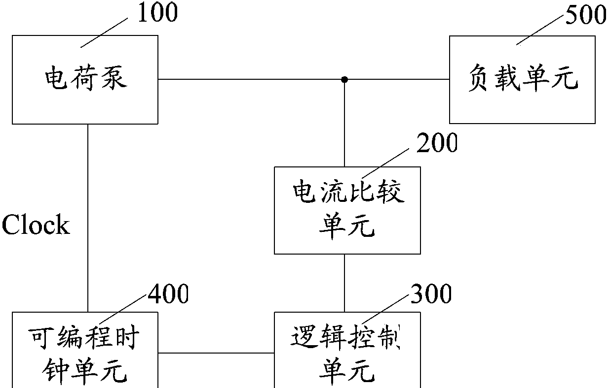
The invention relates to a voltage stabilizing circuit and a voltage stabilizing device. The voltage stabilizing device comprises a charge pump and the voltage stabilizing circuit, wherein the voltage stabilizing circuit comprises a circuit comparison unit, a logic control unit and a programmable clock unit; the current comparison unit is used for converting detected output voltage of the charge pump into current and carrying out comparison on the current and at least two different reference currents to obtain a comparison result; the logic control unit is used for receiving the comparison result and generating a clock-frequency adjusting signal on bases of the comparison result; the programmable logic unit is used for adjusting the frequency of a clock signal according to the received clock-frequency adjusting signal, and sending the clock signal to the charge pump. The voltage stabilizing circuit and the voltage stabilizing device disclosed by the invention have the advantages that due to adoption of the technical scheme, the power consumption of the circuit is effectively reduced, and the reliability of the circuit is improved.
Need to check novelty before this filing date? Find Prior Art

Description

technical field

[0001] The invention relates to the technical field of integrated circuits, in particular to a voltage stabilizing circuit and a voltage stabilizing device. Background technique

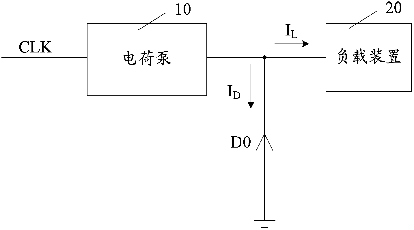
[0002] Electrically Erasable Programmable Read-Only Memory (EEPROM) needs a precise higher voltage when erasing and writing. The traditional method is to use a charge pump to boost the voltage, and add a diode to clamp it. Specifically, refer to figure 1 , the charge pump 10 boosts the voltage under the drive of the clock signal CLK to obtain a high voltage, and the high voltage is used to drive the load device 20 . In order to ensure that the output voltage of the charge pump 10 is in a safe state, a clamping diode D0 is generally connected in parallel with the output terminal of the charge pump 10 . Utilizing the current-voltage characteristics of the reverse breakdown of the clamping diode D0, excess current is discharged from the clamping diode D0, so that the high voltage is ...

Examples

Embodiment Construction

[0020] As mentioned in the background art, traditional charge pumps have defects such as large power consumption, low reliability, and temperature drift. Therefore, other technical solutions have been proposed in the prior art to solve the above problems.

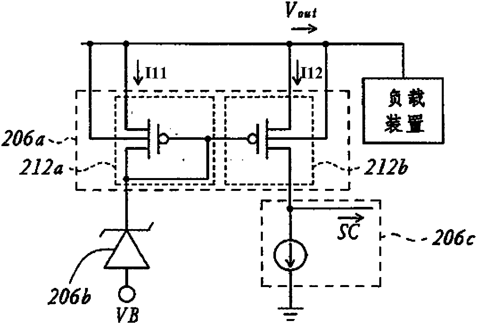
[0021] For example, Chinese patent application No. 200610149595.2 proposes a voltage stabilizing unit using Zener diodes to receive the driving voltage output by the charge pump and control the level of the driving voltage to stabilize the driving voltage. The voltage stabilizing unit includes a current comparison unit, such as figure 2 shown.

[0022] refer to figure 2 , the current comparison unit includes: a current mapping unit 206a, a Zener diode 206b and a bias unit 206c.

[0023] The current mapping unit 206a has a current master control terminal 212a and a current slave terminal 212b. The current mapping unit 206a receives the output voltage Vout, and outputs the voltage Vout as a driving voltage, so as to cont...