High-power semiconductor laser focus indicator used for laser processing

A laser processing and semiconductor technology, applied in laser welding equipment, metal processing equipment, manufacturing tools, etc., can solve problems such as difficult processes and dangerous laser processing operations, and achieve good anti-interference ability, long service life, and easy installation and operation Effect

Inactive Publication Date: 2014-01-29
FOCUSLIGHT TECH
View PDF8 Cites 4 Cited by
  • Summary
  • Abstract
  • Description
  • Claims
  • Application Information

AI Technical Summary

Problems solved by technology

The high-power semiconductor laser processing system is non-visible light, which is more dangerous when performing laser processing operations. At the same time, it is difficult to adjust the process because it is invisible.

Method used


Image

  • High-power semiconductor laser focus indicator used for laser processing
  • High-power semiconductor laser focus indicator used for laser processing
  • High-power semiconductor laser focus indicator used for laser processing

Examples


Embodiment Construction

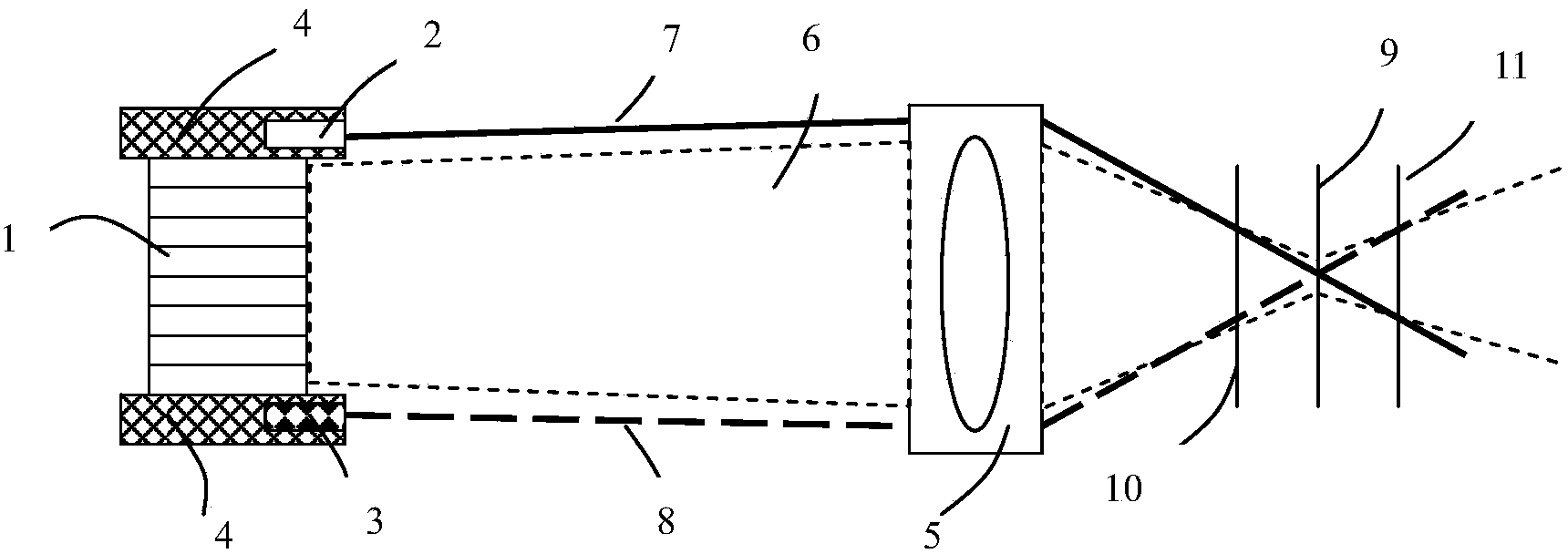
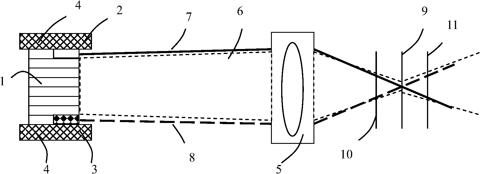
[0021] like figure 1 , figure 2 As shown, during laser processing, before turning on the high-power stacked laser, it is necessary to indicate the exact position of the stacked spot, so that the processing can be carried out accurately. The present invention adopts the method of installing indicating light sources with the same or different wavelengths on both sides of the stack to realize the determination of the spot position of the stack and the judgment of positive and negative defocus. The specific implementation is as follows:

[0022] The two indicating light sources are respectively installed on both sides of the stack, so that their beams intersect at the focal point of the stack laser after passing through the same optical shaping module as the stack laser. If the light spot of indicating light source a does not coincide with the light spot of indicating light source b, it means that the object to be processed is not at the focal point of the array of light spots, ...


PUM


Abstract

The invention provides a high-power semiconductor laser focus indicator used for laser processing, which can improve alignment precision of a semiconductor laser efficiently and increase processing efficiency. The high-power semiconductor laser focus indicator used for laser processing comprises a semiconductor laser stack and an optical shaping module, wherein the semiconductor laser stack or the optical shaping module is provided with more than two indicating light sources which can be distinguished by naked eyes, and a converging point of lights emitted by the indicating light sources after passing through the optical shaping module is located at a light spot focus of the semiconductor laser stack.

Description

technical field [0001] The invention belongs to the technical field of laser processing, and relates to an indicator for locating the spot position of a high-power semiconductor laser. Background technique [0002] High-power semiconductor lasers have the advantages of small size, light weight, high efficiency, and long life. They have been widely used in laser processing, laser medical treatment, laser display, and scientific research. A wide range of comprehensive core devices. [0003] Laser processing technology is a high-tech fusion of modern physics, chemistry, computer, material science, advanced manufacturing technology and other multidisciplinary technologies, including laser surface modification technology, laser surface repair technology, laser cladding technology, laser productization technology, etc. , enabling low-grade materials to achieve high-performance surface modification, achieving the best combination of low-cost parts and high-performance working surf...

Claims


Application Information

Patent Timeline
IPC IPC(8): B23K26/04
CPCB23K26/702
Inventor 宋涛刘兴胜王敏景彩云顾维一程宁蔡磊
Owner FOCUSLIGHT TECH
Why Eureka
Try Eureka