Piezoelectric strain sensor, method for testing strain sensitivity of piezoelectric strain sensor and application of piezoelectric strain sensor
A strain sensor and testing method technology, applied in the measurement of the property force of the piezoelectric resistance material, the calibration/testing of the force/torque/power measuring instrument, instruments, etc., to achieve stable performance, good mechanical compatibility, and electromagnetic resistance strong interference effect
- Summary
- Abstract
- Description
- Claims
- Application Information
AI Technical Summary
Problems solved by technology
Method used
Image
Examples
Embodiment 1
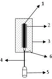
[0047] Piezoelectric strain sensor of the present invention such as figure 1 As shown, the PZT piezoelectric ceramic sheet (thickness 1mm) is used as the piezoelectric sensing element. The upper surface of the piezoelectric ceramic sheet is the positive electrode, and the lower surface is the negative electrode. The positive and negative electrodes are connected with shielding wires, and there is a layer of A 0.5mm thick silicone layer, with an encapsulation layer attached to the piezoelectric ceramic sheet and the silicone layer. As the outermost layer of the sensor, the packaging layer isolates the piezoelectric ceramic sheet from the outside world. The silica gel layer and the piezoelectric ceramic sheet are in direct contact with the packaging layer, so that the piezoelectric ceramic sheet is evenly stressed. In addition, the shielding wire is drawn from the negative electrode of the piezoelectric ceramic sheet, the end of the shielding wire is pasted on the outer surface...
Embodiment 2
[0051] Prepare according to the method for embodiment 1 figure 1 The structure of the sensor, the difference is: the encapsulation layer material is a mixture of sulfoaluminate cement, AB-grouting resin, curing agent and graphite with a mass ratio of 4:4:1:2; the thickness of the encapsulation layer is 1.5mm.
Embodiment 3
[0053] Prepare according to the method for embodiment 1 figure 1 The structure of the sensor, the difference is: the material of the encapsulation layer is a mixture of sulfoaluminate cement, AB-grouting resin, curing agent and graphite with a mass ratio of 4:4:1:3; the thickness of the encapsulation layer is 1.5mm.
PUM
| Property | Measurement | Unit |
|---|---|---|
| thickness | aaaaa | aaaaa |
| thickness | aaaaa | aaaaa |
| thickness | aaaaa | aaaaa |
Abstract
Description
Claims
Application Information


