Conductive substrate and touch panel

一种导电基板、触控面板的技术,应用在电气元件、印刷电路、电数字数据处理等方向,能够解决座标信号无法利用电压差等问题,达到降低视觉干扰、提升视觉效果、解决误差的效果

Active Publication Date: 2014-02-12
WISTRON CORP
View PDF5 Cites 1 Cited by
  • Summary
  • Abstract
  • Description
  • Claims
  • Application Information

AI Technical Summary

Problems solved by technology

In this way, the coordinate signal representing the touch input generated by the signal processing module 14 cannot use the characteristics of the voltage difference to accurately and quickly reflect the position of the touch input, which will lead to the correctness of subsequent signal processing and application.

Method used


Image

  • Conductive substrate and touch panel
  • Conductive substrate and touch panel
  • Conductive substrate and touch panel

Examples


Embodiment Construction

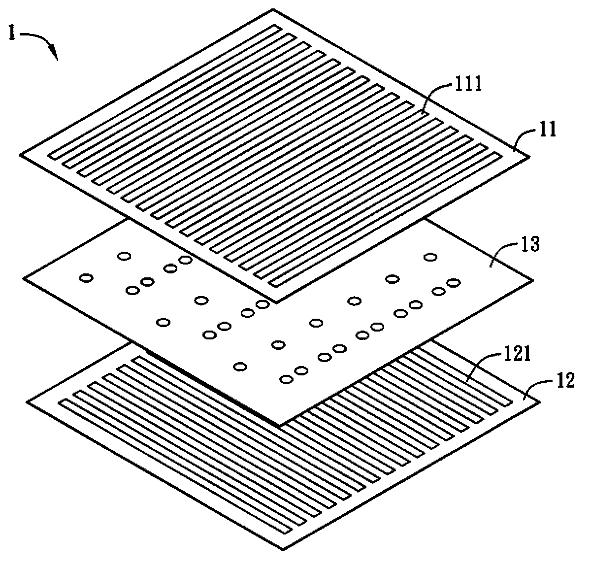
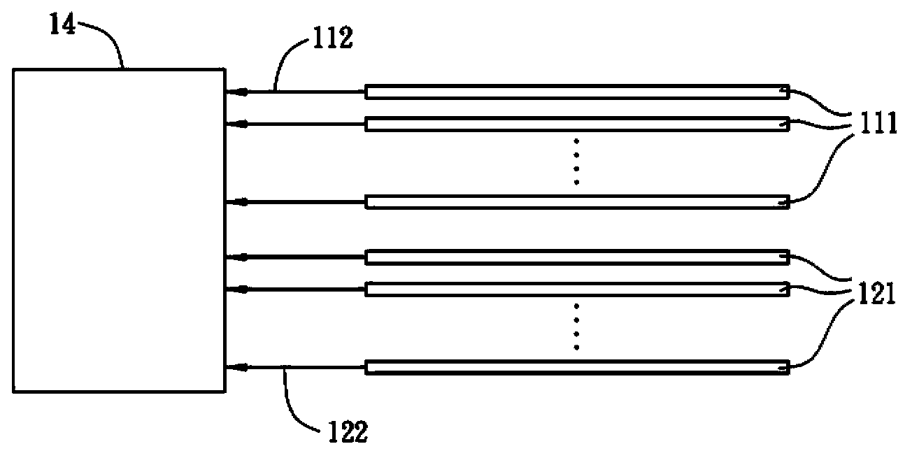
[0075] A conductive substrate and a touch panel according to preferred embodiments of the present invention will be described below with reference to related drawings, wherein the same elements will be described with the same reference symbols.

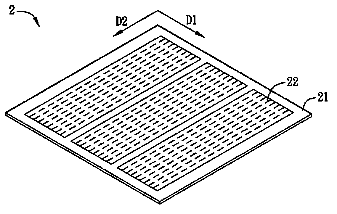
[0076] First, please refer to Figure 2A and Figure 2B As shown, it is a schematic diagram of a conductive substrate 2 in a preferred embodiment of the present invention. The conductive substrate 2 includes a substrate 21 , a plurality of conductive regions 22 , a plurality of first conductive lines 23 , a plurality of conductive pads 24 and a plurality of second conductive lines 25 . In this embodiment, the conductive substrate 2 is a touch substrate applied to a display panel. The conductive substrate 2 is preferably applied to a touch panel, and will be described below as an example.

[0077] The substrate 21 can be a transparent substrate, such as a plastic substrate or a glass substrate. Of course, the substrate 21 can also b...


PUM


Abstract

A conductive substrate includes a substrate, a plurality of conductive areas, a plurality of first conductive wires, a plurality of conductive pads and a plurality of second conductive wires. The conductive areas are disposed on the substrate along a first direction in sequence. The conductive areas are formed and have a plurality of extending conductive portions along a second direction. The conductive portions of two of the adjacent conductive areas are disposed interlacedly. One terminal of each of the first conductive wires is electrically connected to one of the conductive areas. Each of the conductive pads is electrically connected to other terminal of one of the first conductive wires. One terminal of each of the second conductive wire is electrically connected to one of the conductive pads. In addition, a touch panel is also disclosed in the present invention.

Description

technical field [0001] The invention relates to a conductive substrate and a touch panel. Background technique [0002] Various types of touch input technologies have been widely used in electronic products. For example, mobile phones and tablet computers use touch panels as input interfaces. Users can conveniently place their hands directly on the surface of the input panel to issue instructions, or Move around on the surface of the touch panel to operate the mouse or input handwritten characters. The display panel matched with the touch panel can also display virtual buttons for the user to click, and the user can input corresponding relevant text through these virtual buttons. [0003] Such as Figure 1A and Figure 1B As shown, it is a schematic diagram of a conventional touch panel 1 . The touch panel 1 includes a first substrate 11 , a second substrate 12 and a spacer layer 13 . Wherein, a plurality of first electrodes 111 are disposed on the first substrate 11 to ...

Claims


Application Information

Patent Timeline
Patent Type & Authority Applications(China)
IPC IPC(8): G06F3/041G06F3/045
CPCG06F3/045G06F2203/04103H05K1/111
Inventor 王贵璟林达湖
Owner WISTRON CORP
Why Eureka
Try Eureka