Waxed polishing method for reducing chemical burns of single crystal silicon polished wafer

A technology for chemical burns and polishing sheets, which is applied to chemical instruments and methods, cleaning methods using tools, cleaning methods using liquids, etc., to achieve good matching of chemical effects, improve process parameters, and reduce chemical burns

Active Publication Date: 2014-03-26
ZHONGHUAN ADVANCED SEMICON MATERIALS CO LTD +1
View PDF7 Cites 2 Cited by
  • Summary
  • Abstract
  • Description
  • Claims
  • Application Information

AI Technical Summary

Problems solved by technology

[0005] The purpose of the present invention is to solve the problems existing in the existing polishing technology by improving the cleaning circulation system of the polishing soluti...

Method used


Image

  • Waxed polishing method for reducing chemical burns of single crystal silicon polished wafer
  • Waxed polishing method for reducing chemical burns of single crystal silicon polished wafer
  • Waxed polishing method for reducing chemical burns of single crystal silicon polished wafer

Examples


Embodiment 1

[0032] Experimental material: 6-inch heavily doped silicon wafer to be thrown, resistivity 0.008-0.02Ω·cm 2 , the thickness is 625±15μm, and the quantity is 192 pieces.

[0033] Processing equipment: wax single-sided polishing system (including one waxing machine, two rough polishing machines, one medium polishing machine, one fine polishing machine, one wafer downloading device, one ceramic disc cleaning machine, PTU Ceramic disk transfer device), one JAC cleaning machine after polishing, one pre-cleaning machine, CR81 silicon wafer surface particle tester.

[0034] Auxiliary materials: ceramic disc, disc brush, polishing pad, coarse polishing liquid, medium polishing liquid, fine polishing liquid, pure water, potassium hydroxide, acetic acid, PFA chip basket, lower chip shovel.

[0035] The parameters of the medium polishing process and the fine polishing process are the same as those in (6) and (7) in the specific implementation steps. The process parameters of the rough p...

Embodiment 2

[0045] Experimental material: 6-inch lightly doped silicon wafer to be thrown, resistivity 2-10Ω·cm 2 , the thickness is 510±10μm, and the quantity is 192 pieces.

[0046] Processing equipment: wax single-sided polishing system (including one waxing machine, two rough polishing machines, one medium polishing machine, one fine polishing machine, one wafer downloading device, one ceramic disc cleaning machine, PTU Ceramic disk transfer device), one JAC cleaning machine after polishing, one pre-cleaning machine, CR81 silicon wafer surface particle tester.

[0047] Auxiliary materials: ceramic disc, disc brush, polishing pad, coarse polishing liquid, medium polishing liquid, fine polishing liquid, pure water, potassium hydroxide, acetic acid, PFA chip basket, lower chip shovel.

[0048] The parameters of the medium polishing process and the fine polishing process are the same as those in (6) and (7) in the specific implementation steps. The process parameters of the rough polishi...

Embodiment 3

[0052] Experimental material: 5-inch lightly doped silicon wafer to be thrown, resistivity 3000-8000Ω·cm 2 , the thickness is 400±10μm, and the quantity is 192 pieces.

[0053] Processing equipment: wax single-sided polishing system (including one waxing machine, two rough polishing machines, one medium polishing machine, one fine polishing machine, one wafer downloading device, one ceramic disc cleaning machine, PTU Ceramic disk transfer device), one JAC cleaning machine after polishing, one pre-cleaning machine, CR81 silicon wafer surface particle tester.

[0054] Auxiliary materials: ceramic disc, disc brush, polishing pad, coarse polishing liquid, medium polishing liquid, fine polishing liquid, pure water, potassium hydroxide, acetic acid, PFA chip basket, lower chip shovel.

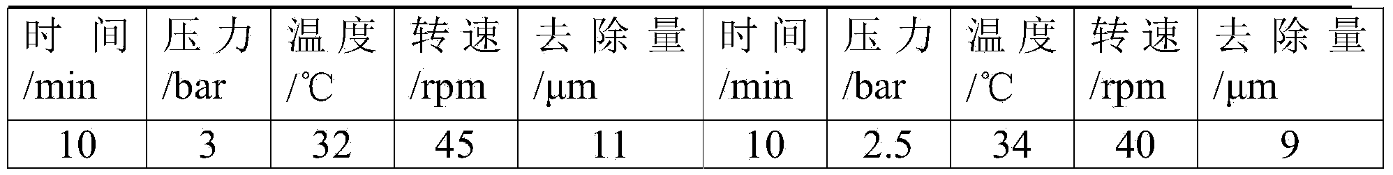
[0055] The process parameters are shown in the table below:

[0056]

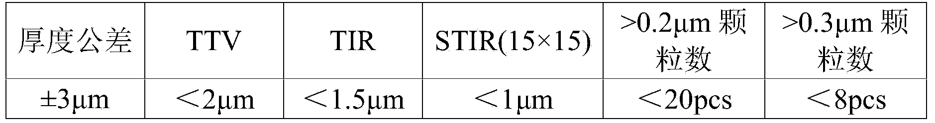
[0057] Through the detection, it is concluded that the quality parameters of the 5-inch lightly doped silicon wafer process...


PUM


Abstract

The invention provides a waxed polishing method for reducing chemical burns of a single crystal silicon polished wafer. The polishing method comprises the three working procedures of cleaning polishing tools, uploading a polishing machine to carry out polishing, and cleaning a doped silicon wafer which is polished. The necessary neutralization process is added on the basis of the process of cleaning a polishing liquid barrel in the prior art, the process parameters in the polishing process are improved at the same time, polishing mechanical strength and the chemical function in the polishing process are matched well, and therefore the chemical burns of a polished surface of the silicon wafer are reduced, the purpose that the chemical burns of the polished surface are smaller than or equal to 0.1% is achieved, and the silicon wafer with the perfect polished surface is obtained.

Description

technical field [0001] The invention relates to the field of semiconductor polishing technology, in particular to a wax polishing method for reducing chemical burns of a single crystal silicon wafer polishing sheet. Background technique [0002] The surface condition is a key indicator of silicon polished wafers, which is directly related to the yield rate of the final device product. During the processing, each process must be carried out according to the technical requirements, and polished under a reasonable chemical-mechanical interaction. Qualified silicon polishing wafers have high requirements for surface flatness, strict requirements for surface particle size, perfect surface conditions, and no surface defects such as burns and orange peels are allowed. Therefore, in the polishing process, the chemical mechanical action must be well matched and easy to control, and the quality of the polishing pad and liquid must be matched to produce a perfect silicon polishing wafe...

Claims


Application Information

Patent Timeline
IPC IPC(8): B24B1/00B08B3/12B08B1/00
CPCB24B1/00H01L21/02013
Inventor 吕莹魏艳军刘园张晋会李翔
Owner ZHONGHUAN ADVANCED SEMICON MATERIALS CO LTD
Why Eureka
Try Eureka