Display device and repair method thereof and array substrate

An array substrate and substrate substrate technology, which is applied in nonlinear optics, instruments, optics, etc., can solve problems such as the limitation of data line repair, the limited number of repair lines, and the impact on the display effect of display devices.

Active Publication Date: 2014-04-02
HEFEI BOE OPTOELECTRONICS TECH +1
View PDF7 Cites 15 Cited by
  • Summary
  • Abstract
  • Description
  • Claims
  • Application Information

AI Technical Summary

Problems solved by technology

[0005] First, due to the increasing size of liquid crystal display devices, correspondingly longer repair lines need to be arranged on the array substrate, so that the line resistance and line capacitance of the repair lines continue to increase. After forming a path together, the line resistance and line capacitance of the repaired line have a

Method used


Image

  • Display device and repair method thereof and array substrate
  • Display device and repair method thereof and array substrate
  • Display device and repair method thereof and array substrate

Examples


Embodiment Construction

[0032] The technical solutions in the embodiments of the present invention will be clearly and completely described below in conjunction with the accompanying drawings in the embodiments of the present invention. Obviously, the described embodiments are only a part of the embodiments of the present invention, rather than all the embodiments. Based on the embodiments of the present invention, all other embodiments obtained by those of ordinary skill in the art without creative work shall fall within the protection scope of the present invention.

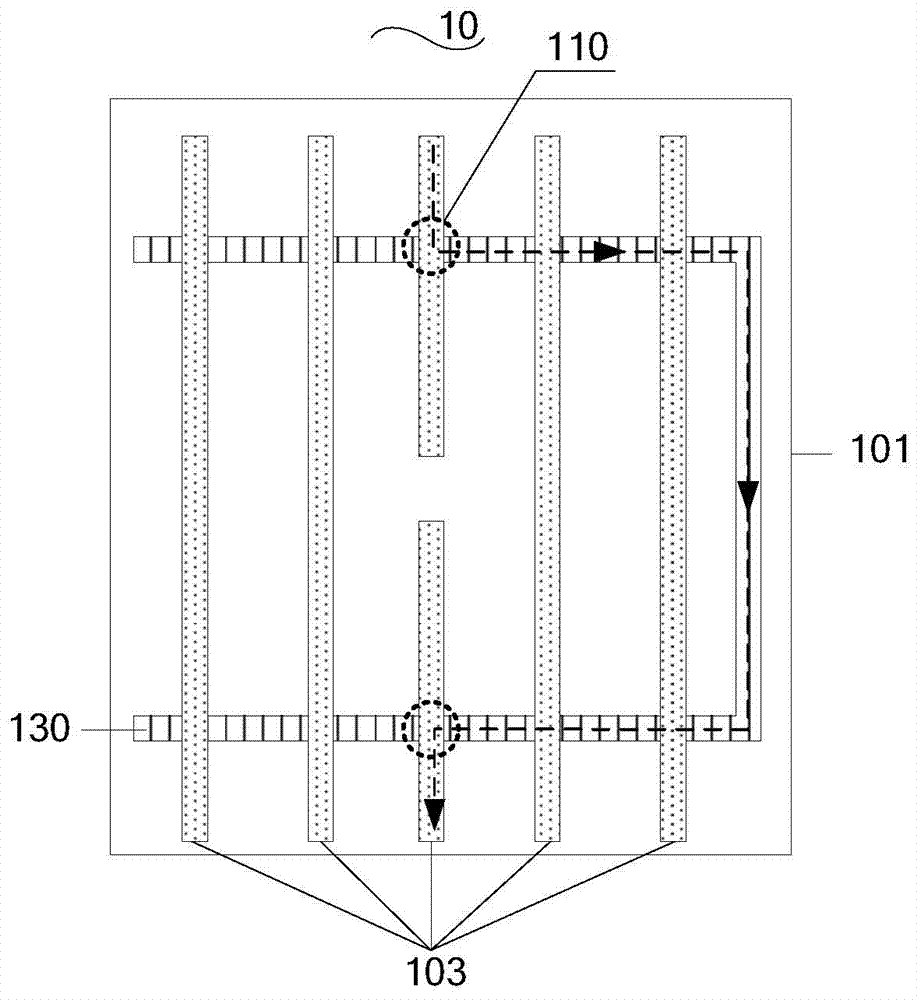
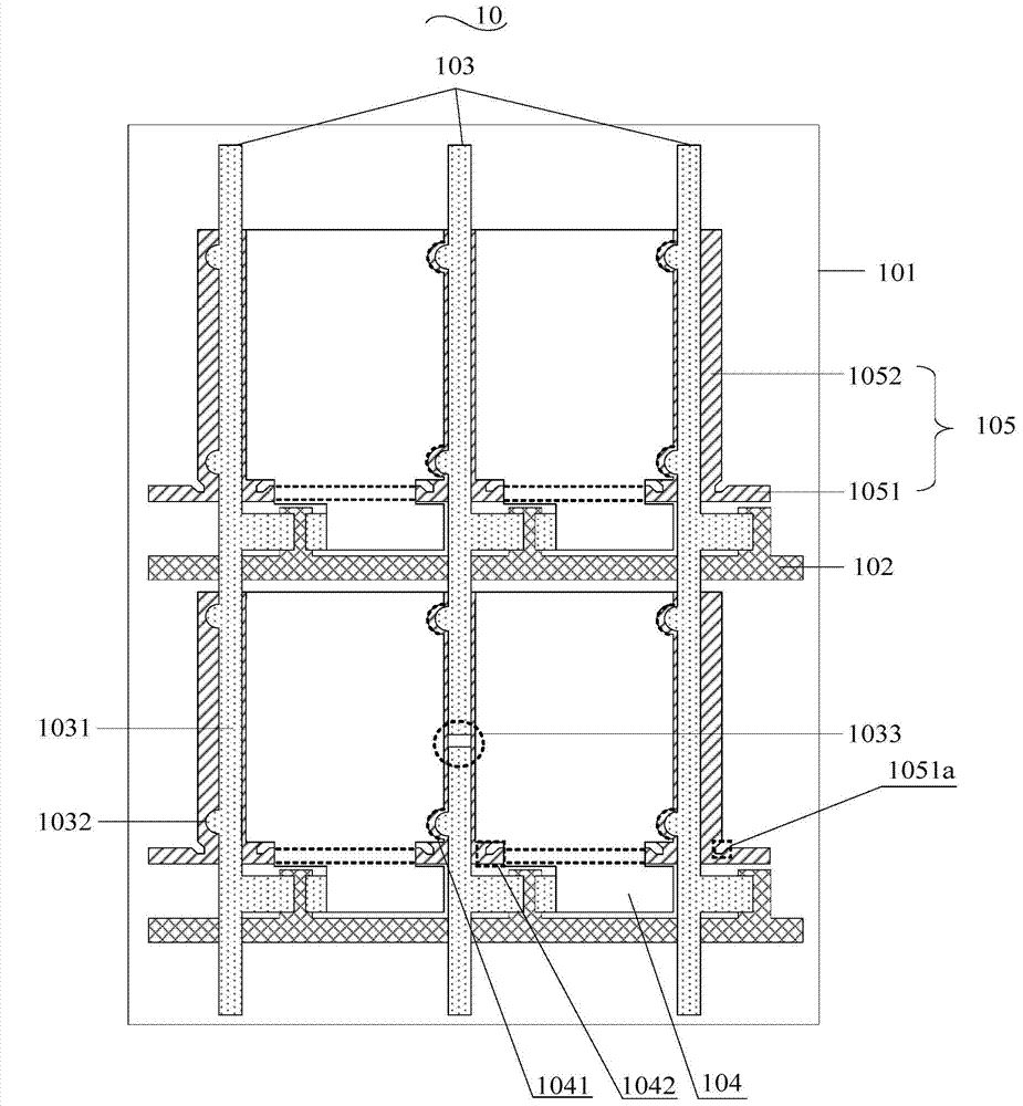
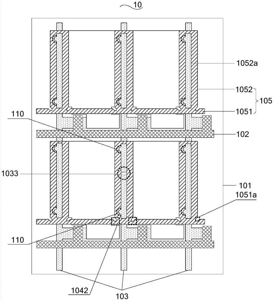
[0033] The embodiment of the present invention provides an array substrate 10, such as Figure 2 ~ Figure 4 As shown, the array substrate 10 includes a base substrate 101, gate lines 102, data lines 103, and pixel electrodes 104 disposed on the base substrate 101; in addition, the array substrate 10 also includes a plurality of conductive electrodes 105 Any one of the conductive electrodes 105 is located between two adjacent gate lines 1...


PUM


Abstract

An embodiment of the invention provides a display device and a repair method thereof and an array substrate and relates to the display technical field and the production of the array substrate and the display device comprising the same. The array substrate comprises an underlayer substrate, grid lines, data lines, pixel electrodes and a plurality of conductive electrodes; the grid lines, the data lines, the pixel electrodes and the plurality of conductive electrodes are arranged on the underlayer substrate; any one of the conductive electrodes is located between the two adjacent grid lines; every conductive electrode comprises a horizontal electrode wire and a plurality of vertical electrode wires; the vertical electrode wires are electrically connected with the horizontal electrode wire and arranged separately; the positions of the vertical electrode wires are corresponding to the positions of the data lines; the data lines comprise the vertical portions and protruding portions in the two adjacent grid lines, wherein the vertical portions are perpendicular to the vertical electrode wires and the protruding portions are connected with the vertical portions and arranged close to the grid lines; the pixel electrodes and the protruding portions and the horizontal electrode wire portions which are close to the bilateral sides of the vertical electrode wires are not overlapped. According to the display device and the repair method thereof and the array substrate, the data line signal loss caused by too long repair lines can be reduced, the data lines cannot be limited by the number of the repair lines, and accordingly the repair efficiency is improved.

Description

Technical field [0001] The present invention relates to the field of display technology, in particular to an array substrate, a display device and a repair method thereof. Background technique [0002] At present, in the manufacturing process of liquid crystal display (Liquid Crystal Display, LCD for short), due to the influence of the substrate surface fluctuation, heat treatment, etching process, etc., the width of the data line in the existing array substrate structure is small, and the data line occurs The probability of data open is relatively high. When the data line is disconnected, the signal cannot be transmitted to the corresponding pixel area, which will cause the liquid crystal display device to fail to display normally. [0003] When the disconnection of the data line is found before the cell formation process of the liquid crystal display device, the broken data line can be repaired by the chemical vapor deposition method. However, due to the high probability of miss...

Claims


Application Information

Patent Timeline
IPC IPC(8): G02F1/1362G02F1/1368G02F1/13G02F1/1343G02F1/1345
Inventor 邓玉新童冉代训体钮曼萍
Owner HEFEI BOE OPTOELECTRONICS TECH
Why Eureka
Try Eureka