Array substrate, display panel and display device

An array substrate and display panel technology, which is applied in the direction of TV, color TV, telephone communication, etc., can solve the problems affecting the wiring arrangement of the array substrate and affecting the performance of electronic devices, etc.

Pending Publication Date: 2020-05-08
HONG FU JIN PRECISION IND (SHENZHEN) CO LTD +1
View PDF2 Cites 3 Cited by
  • Summary
  • Abstract
  • Description
  • Claims
  • Application Information

AI Technical Summary

Problems solved by technology

[0003] Taking an array substrate including multiple wires in an electronic device as an example, the array substrate needs to be provided with a camera hole area exposing

Method used


Image

  • Array substrate, display panel and display device
  • Array substrate, display panel and display device
  • Array substrate, display panel and display device

Examples


Embodiment Construction

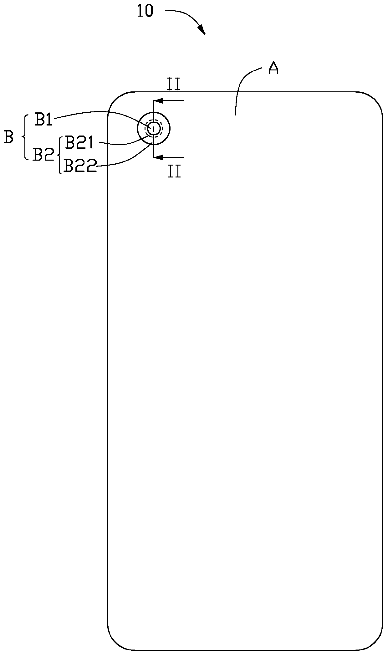
[0081] figure 1 It is a schematic top view of the array substrate 10 according to an embodiment of the present invention. Such as figure 1 As shown, the array substrate 10 defines a display area A and a camera hole area B surrounded by the display area A. As shown in FIG. The camera hole area B defines a light-transmitting area B1 and a wiring area B2 surrounding the light-transmitting area B1. The routing area B2 includes a first routing area B21 adjacent to the transparent area B1 and a second routing area B22 surrounding the first routing area B21. The camera hole area B is a light-transmitting area. The camera hole area B and the transparent area B1 are approximately circular. The routing area B2 is a ring. In other embodiments, the camera hole area B can also have other shapes. For example, oval, polygon, etc.

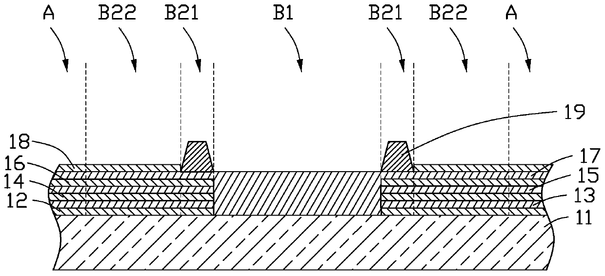
[0082] figure 2 for figure 1 A schematic cross-sectional view taken along the section line II-II. Such as figure 2 As shown, the array substrate 10 inc...


PUM


Abstract

The embodiment of the invention provides an array substrate, a display panel applying the array substrate and a display device. The array substrate defines a display area and a camera hole area surrounded by the display area. The camera hole area comprises a light-transmitting area, a first wiring area adjacent to the light-transmitting area, and a second wiring area surrounding the first wiring area. The array substrate comprises a first substrate, a first conductive layer, a second conductive layer, a common electrode layer, a third conductive layer, a planarization layer and an optical spacer. And the area of the planarization layer, which is aligned with the light-transmitting area, is in direct contact with the first substrate. The optical spacer is arranged to be aligned with the first wiring area. And the third conductive layer is arranged by bypassing the light-transmitting area and the first wiring area.

Description

technical field [0001] The present invention relates to the field of display technology, and in particular to an array substrate, a display panel using the array substrate, and a display device using the display panel. Background technique [0002] Electronic devices, such as mobile phones, tablet computers, etc., often need to be combined with components with other functions as users have increasing demands for diversified functions. Among them, electronic devices combined with camera modules have been widely produced and applied. [0003] Taking an array substrate including multiple wires in an electronic device as an example, the array substrate needs to be provided with a camera hole area exposing the camera module. However, the camera hole area will affect the arrangement of the wires on the array substrate, and even affect the performance of the electronic device. . Contents of the invention [0004] One aspect of the present invention provides an array substrate, ...

Claims


Application Information

Patent Timeline
IPC IPC(8): G02F1/1339G02F1/1362G02F1/1368H04N5/225
CPCG02F1/13394G02F1/136286G02F1/1368G02F1/13398H04N23/57G06F3/0412G06F3/04166G06F3/0446G06F1/1686G06F1/1637G06F1/1626H04M1/0266H04M1/0264H01L27/124G02F1/13338G03B30/00H10K59/65H10K59/40H10K59/131G02F1/133388G02F1/133357G02F1/133512G02F1/133514G02F1/133602
Inventor 欧阳祥睿陈维成
Owner HONG FU JIN PRECISION IND (SHENZHEN) CO LTD
Why Eureka
Try Eureka