Method for forming metal gate

A metal gate and metal layer technology, which is applied in the direction of electrical components, semiconductor/solid-state device manufacturing, semiconductor devices, etc., can solve the problems of metal gate resistivity change, semiconductor device failure, etc., to improve the sag situation and prevent thickness change Small, the effect of improving electrical performance and reliability

Active Publication Date: 2014-04-02
SEMICON MFG INT (SHANGHAI) CORP +1
View PDF3 Cites 0 Cited by
  • Summary
  • Abstract
  • Description
  • Claims
  • Application Information

AI Technical Summary

Problems solved by technology

For example, to form an aluminum metal gate with a total height of 400-600 angstroms, a 300 angstrom recess makes the thickness of the aluminum metal gate smaller, causing a serious change in the resistivity of the metal gate, resulting in failure of the semiconductor device

Method used


Image

  • Method for forming metal gate
  • Method for forming metal gate
  • Method for forming metal gate

Examples


no. 1 example

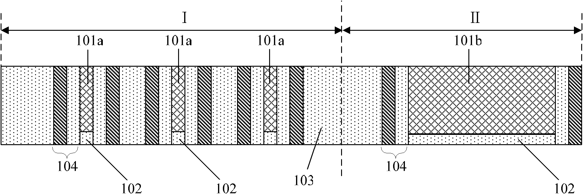
[0039] Figure 6 to Figure 15 It is a schematic cross-sectional view of the first embodiment of the metal gate forming method of the present invention. Such as Figure 6As shown, a semiconductor substrate 200 is provided; the surface area of ​​the semiconductor substrate 200 is divided into a core unit area I and a peripheral circuit area II; a sacrificial oxide layer 202 and a polysilicon gate 201 are sequentially formed on the semiconductor substrate 200 . Among them, in the core cell area I, due to the high device density, there are relatively many polysilicon gates 201a, and the critical dimension of the polysilicon gates 201a is relatively small; in the peripheral circuit area II, due to the low device density, the polysilicon gates 201b is relatively sparse, and the key size is relatively large. The specific process of forming the polysilicon gate 201a, 201b is as follows: form a sacrificial oxide layer 202 on the semiconductor substrate 200 by chemical vapor depositio...

no. 2 example

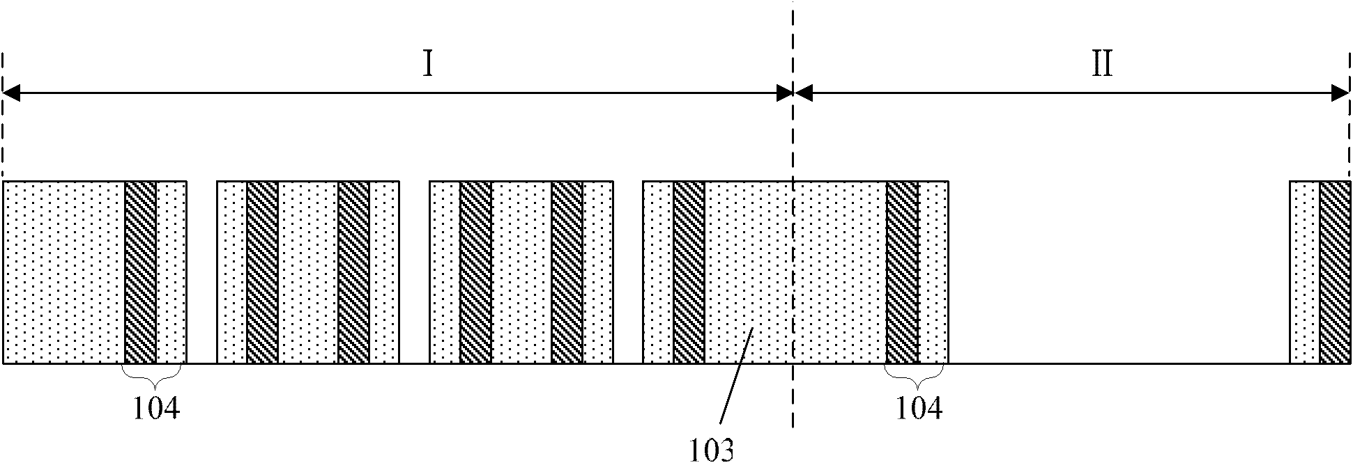
[0056] Figure 16 to Figure 25 It is a schematic cross-sectional view of the second embodiment of the metal gate forming method of the present invention. Such as Figure 16 As shown, a semiconductor substrate 300 is provided; the surface area of ​​the semiconductor substrate 300 is divided into a core unit area I and a peripheral circuit area II; a sacrificial oxide layer 302 and polysilicon gates 301a, 301b are formed on the semiconductor substrate 300 . Among them, the core cell area I has more polysilicon gates 301a due to the high density of devices, and the critical dimensions of the polysilicon gates 301a are smaller; the peripheral circuit area II has fewer polysilicon gates 301b because of the lower density of devices, and the critical dimensions Also larger. The specific process of forming the polysilicon gates 301a and 301b is as described in the first embodiment.

[0057] Such as Figure 17 As shown, sidewalls 303 are formed on the semiconductor substrate 300 on...


PUM


Abstract

The invention relates to a method for forming a metal gate. The method comprises the following steps of: providing a semiconductor substrate, wherein the semiconductor substrate is divided into a core unit area and a peripheral circuit area, sacrificial oxide layers and dummy gates are formed on the semiconductor substrate in turn, spacers are formed on the semiconductor substrate on the two sides of each dummy gate, and interlayer dielectric (ILD) layers are formed on the semiconductor substrate and flush with the tops of the dummy gates and the spacers; removing the dummy gates and the sacrificial oxide layers to form grooves; forming metal layers on the ILD layers, and filling the grooves; forming protection layers in the groove of the peripheral circuit area and the metal layer on the edge of the groove; and grinding the protection layers and the metal layers until the ILD layers are exposed to form the metal gate, wherein the grinding rate of the protection layers is lower than that of the metal layers. By the method, the defect that the metal gate is sunken is overcome, and the electrical property of the metal gate and the reliability of a semiconductor device are improved.

Description

technical field [0001] The invention relates to a semiconductor manufacturing process, in particular to a method for forming a metal gate. Background technique [0002] At present, semiconductor chip manufacturing has developed to a process of 32 nanometers and below, and the traditional polysilicon gate can no longer meet the electrical performance requirements under this feature size. In order to solve the serious leakage current and power consumption problems caused by the traditional polysilicon gate, for the process of 32 nanometers and below, most of the current high dielectric constant (high-k) dielectric materials are used as the gate dielectric layer, and metal materials are used as the gate. to obtain good electrical properties. The manufacturing process for the metal gate is as disclosed in US Patent US20100052070: first form a high-k dielectric layer on the semiconductor substrate, and deposit a conductive layer on the high-k dielectric layer; use polysilicon to...

Claims


Application Information

Patent Timeline
Patent Type & Authority Patents(China)
IPC IPC(8): H01L21/28H01L21/285
Inventor 蒋莉黎铭琦
Owner SEMICON MFG INT (SHANGHAI) CORP
Why Eureka
Try Eureka