High selectivity and high planarity dielectric polishing

a dielectric and high selectivity technology, applied in the direction of other chemical processes, polycrystalline material growth, crystal growth process, etc., can solve the problems of large device area stress, reduced device efficiency, and reduced device efficiency, so as to achieve high selectivity and high planarity the effect of high efficiency and rapid removal of materials

Inactive Publication Date: 2005-03-15
UNIV OF FLORIDA
View PDF8 Cites 44 Cited by
  • Summary
  • Abstract
  • Description
  • Claims
  • Application Information

AI Technical Summary

Benefits of technology

During polishing of the silicon dioxide or low K dielectric layer, the silicon dioxide or low K dielectric surface can be efficiently planarized due to non-substantial or substantial adsorption of the additive, depending on the pressure applied in the polishing process. High planarization efficiency can result from non-linear polishing characteristics of silicon dioxide or low K material or similar materials as a function of pressure. At relatively high points in the circuit topography where the pressure is high, rapid removal of the material takes place. In contrast, in low topographical areas where the pressure is lower, slower removal of the material takes place. This process results in rapid planarization of the silicon dioxide or low K dielectric film when compared to conventional slurries which typically show linear removal rates as a function of pad pressure.
When pressure dependent polishing is used to form silicon dioxide

Problems solved by technology

The combined layers of neighboring devices can form parasitic devices.
One disadvantage of the LOCOS process is that the silicon dioxide (isolation layer) grows in an isotropic manner resulting in consumption of the surface area of the semiconductor substrate and causes adjacent electronic devices that are isolated from one another to be a fixed minimum distance apart.
This limits the maximum density of the electronic devices on each microchip.
Additionally, the oxidation of the silicon surface can lead to large stresses in the device area (e.g. bird's beak), which may not be conducive for higher levels on integration demanded by each generation of devices.
Because of the widely varying surface morphologies across the wafer, it is difficult to use a direct CMP process to remove the overburden of silicon dioxide from the surface of a patterned STI wafer.
This effect can cause damage to the thin high-density isolated regions of trenches, while sometimes not removing the oxide in the less dense regions of the substrate.
Damage occurs in isolated regions because the oxide in the area with a large percentage of trenches polishes at a much higher rate than the oxide over the nitride.
CMP induced damage can cause silicon defects which can significantly increase junction leakage and make the wafer unsuitable for production.
The low removal rate of silicon nitride compared to silicon dioxide is sufficient to stop the CMP process before significant removal of the nitride overlayer takes place and damage occurs.
Accordingly, the extra lithographic step increases cycle time, increases the cost of manufacturing, and adds defect density.
Although there is an increase in selectivity, this increase in selectivity is not hig

Method used


Image

  • High selectivity and high planarity dielectric polishing
  • High selectivity and high planarity dielectric polishing
  • High selectivity and high planarity dielectric polishing

Examples


example i

Substantial Adsorption Effect for Silicon Nitride

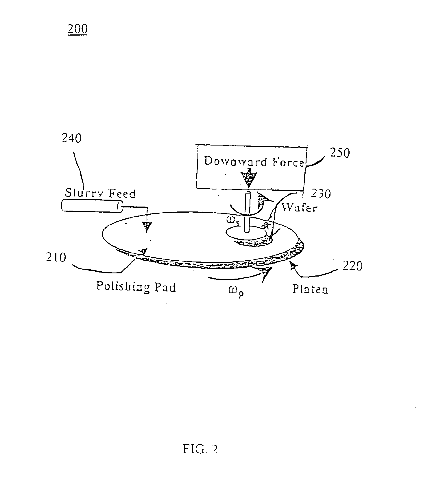
FIG. 15 is a table showing the removal rate of silicon nitride and its adsorption ratio (AR) when a single surfactant and a silicon nitride particle based slurry was used. The CMP experiments were conducted with silicon nitride based slurries at a pH of 3.0, a polishing pressure of 6.7 Psi, and a linear velocity of 253 ft / min. A bench-top Rotopol 30 polisher manufactured by Struer Company was used in this experiment. The concentration of the silicon nitride particles in the slurry was fixed at 2 wt percent. The particle size was varied from 80 nm to 2000 nm. FIG. 15 shows that the substantial adsorption effect can take place when cationic (CTAB), anionic (SDS), or zwitterionic (KETJENLUBE 522® / Dapral GE 202) surfactants are added to slurry.

The removal rate of the silicon nitride is substantially decreased by the addition of the surfactant, thus leading to a high adsorption ratio (AR). A high AR also leads to enhanced selectivity of si...

example ii

Substantial and Non-Substantial Adsorption, and Pressure Dependent Adsorption on Silicon Dioxide

Besides substantial adsorption onto silicon nitride, one preferred embodiment of the invention relates to creating substantial and non-substantial adsorption on silicon dioxide surfaces by addition of specific additives such as surfactants, soluble polymers and salts. Additionally, pressure dependent adsorption effects have also been demonstrated.

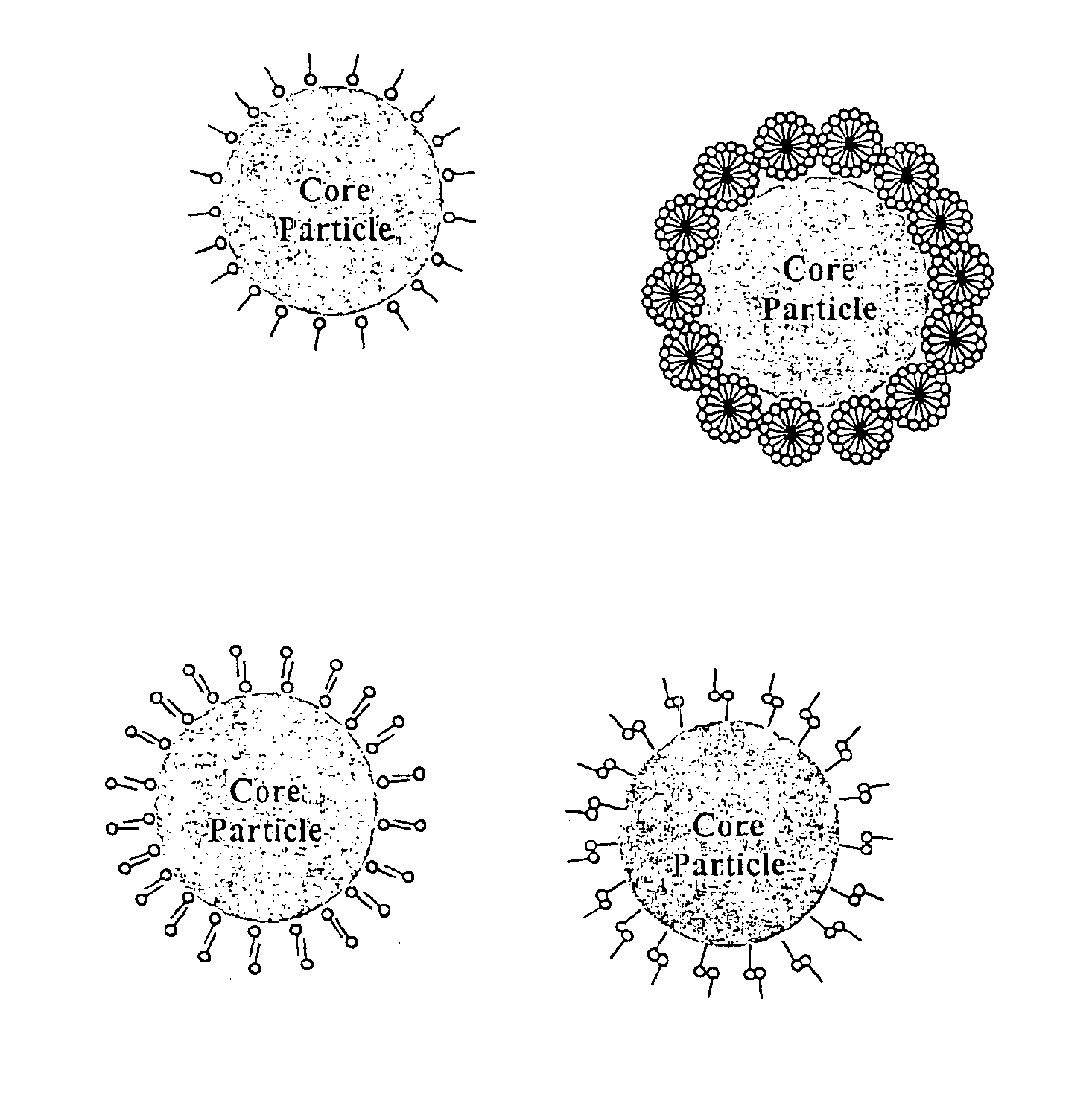
FIG. 19 shows the adsorption ratio on silicon dioxide and carbon doped silica based low K materials using a slurry including CTAB based surfactant additives and various particles. The pH of the slurry was adjusted to 7.0 and the concentration of the particles was varied from 2 to 5 wt. %. The polishing pressure was 6.7 Psi while the linear velocity was 253 ft / sec. Single phase inorganic cores (silicon nitride, silica, and nanoporous silica) and coated inorganic cores (silica coated with ceria, titania, manganese oxide, and alumina coated with sil...

example iii

Selective Adsorption Ratio and Selectivity

By controlling the adsorption ratio for both silicon nitride and silicon dioxide or low K dielectric surfaces, the selective adsorption ratio and the selectivity for polishing silicon dioxide or low K dielectrics with respect to silicon nitride can be controlled. FIG. 23 shows SAR and selectivity values for silicon nitride / silicon dioxide polishing using single and mixed selective adsorption additives. The pH of the slurry in these experiments was kept at 3, while the polishing pressure and the linear velocity were maintained at 6.7 Psi and 250 ft / min, respectively. The particle loading was maintained at 2 weight percent. The concentration of each of the surfactants, polymer additives and salts were varied from 0.1 mM to 128 mM, while the total concentration of surfactant species was 130 mM. The result shows that high SAR values can be obtained using single or a mixture of surfactants / polymer additives and salts.

The SAR values are also gener...


PUM


Abstract

A slurry includes a plurality of particles and at least one selective adsorption additive. The particles are preferably composite particles including a core surrounded by a shell provided by the selective adsorption additive. The slurry can be used to polish a structure including silicon dioxide or a low K dielectric film and a silicon nitride containing film, such as to form a shallow trench isolation (STI) structure or a metal-dielectric structure. The silicon nitride containing film surface substantially adsorbs the selective adsorption additive, whereas the silicon dioxide or low K dielectric film shows non-substantial adsorption characteristics to the adsorption additive. In another embodiment of the invention, silicon dioxide or low K dielectric film shows non-substantial adsorption of the selective adsorption additive at a pressure above a predetermined first pressure, and substantial adsorption of the selective adsorption additive for pressures below a predetermined second pressure, where the first pressure is greater than the second pressure.

Description

STATEMENT REGARDING FEDERALLY SPONSORED RESEARCH OR DEVELOPMENTNot applicable.FIELD OF THE INVENTIONThis invention relates to a slurry and method for chemical-mechanical polishing (CMP) of dielectrics. The slurry can be used in a chemical mechanical planarization step for integrated shallow trench isolation (STI) processes, chip interconnect dielectric planarization, or a variety of dielectric planarization processes.BACKGROUNDReductions in semiconductor device dimensions provide higher densities and improved performance for integrated circuits. In many integrated electronic devices, millions of discrete elements, such as transistors, resistors and capacitors are built in close proximity and integrated onto a single device. The combined layers of neighboring devices can form parasitic devices. Thus, one of the important initial steps in the fabrication of semiconductor devices is to electrically isolate adjacent electronic devices on a common substrate.Isolation structures are gener...

Claims


Application Information

Patent Timeline
IPC IPC(8): C09K13/04C09K13/06C09K13/00C30B21/02C30B7/00C30B21/00C30B28/00C30B28/06H01L21/4763H01L21/02H01L21/302H01L21/461C09G1/02C09K3/14H01LH01L21/3105H01L21/321
CPCC09G1/02C09K3/1463C30B7/005H01L21/3212C30B7/00H01L21/31053
Inventor SINGH, RAJIV K.
Owner UNIV OF FLORIDA
Why Eureka
Try Eureka