Method of planarizing substrate and method of manufacturing thin film transistor using the same

a technology of thin film transistor and substrate, which is applied in the direction of transistors, semiconductor devices, electrical appliances, etc., can solve the problems of deteriorating display quality and reducing and achieve the effect of improving the reliability of display devices and improving the display quality of display devices

Active Publication Date: 2015-07-28
SAMSUNG DISPLAY CO LTD
View PDF13 Cites 0 Cited by
  • Summary
  • Abstract
  • Description
  • Claims
  • Application Information

AI Technical Summary

Benefits of technology

[0008]A method of planarizing a substrate by forming a protruded portion on a conductive pattern to effectively planarize the substrate is provided.
[0010]The method includes forming a conductive pattern on a first surface of a base substrate, forming a positive photoresist layer on the base substrate and the conductive pattern, exposing the positive photoresist layer to light by irradiating a second surface of the base substrate opposite to the first surface with light, developing the positive photoresist layer to form a protruded portion on the conductive pattern, forming a planarizing layer on the base substrate and the protruded portion and eliminating the protruded portion.
[0037]According to the method of planarizing a substrate and the method of manufacturing a TFT, the protruded portion is formed by a back exposure process so that a planarizing characteristic of layer may be improved.
[0038]Thus, the reliability of a display apparatus may be improved and the display quality of the display apparatus may be improved.

Problems solved by technology

When an upper surface of a layer is uneven, a pattern formed on the uneven surface may have a portion that is disconnected, so that the reliability of the display apparatus may decrease.
In addition, when the array substrate and the opposite substrate are not planarized, the cell gap between the array substrate and the opposite substrate is not uniform, so that a stain may be generated on the display panel.
Thus, the display quality of the display apparatus may be deteriorated.

Method used


Image

  • Method of planarizing substrate and method of manufacturing thin film transistor using the same
  • Method of planarizing substrate and method of manufacturing thin film transistor using the same
  • Method of planarizing substrate and method of manufacturing thin film transistor using the same

Examples


Embodiment Construction

[0057]Hereinafter, exemplary embodiments will be described in further detail with reference to the accompanying drawings.

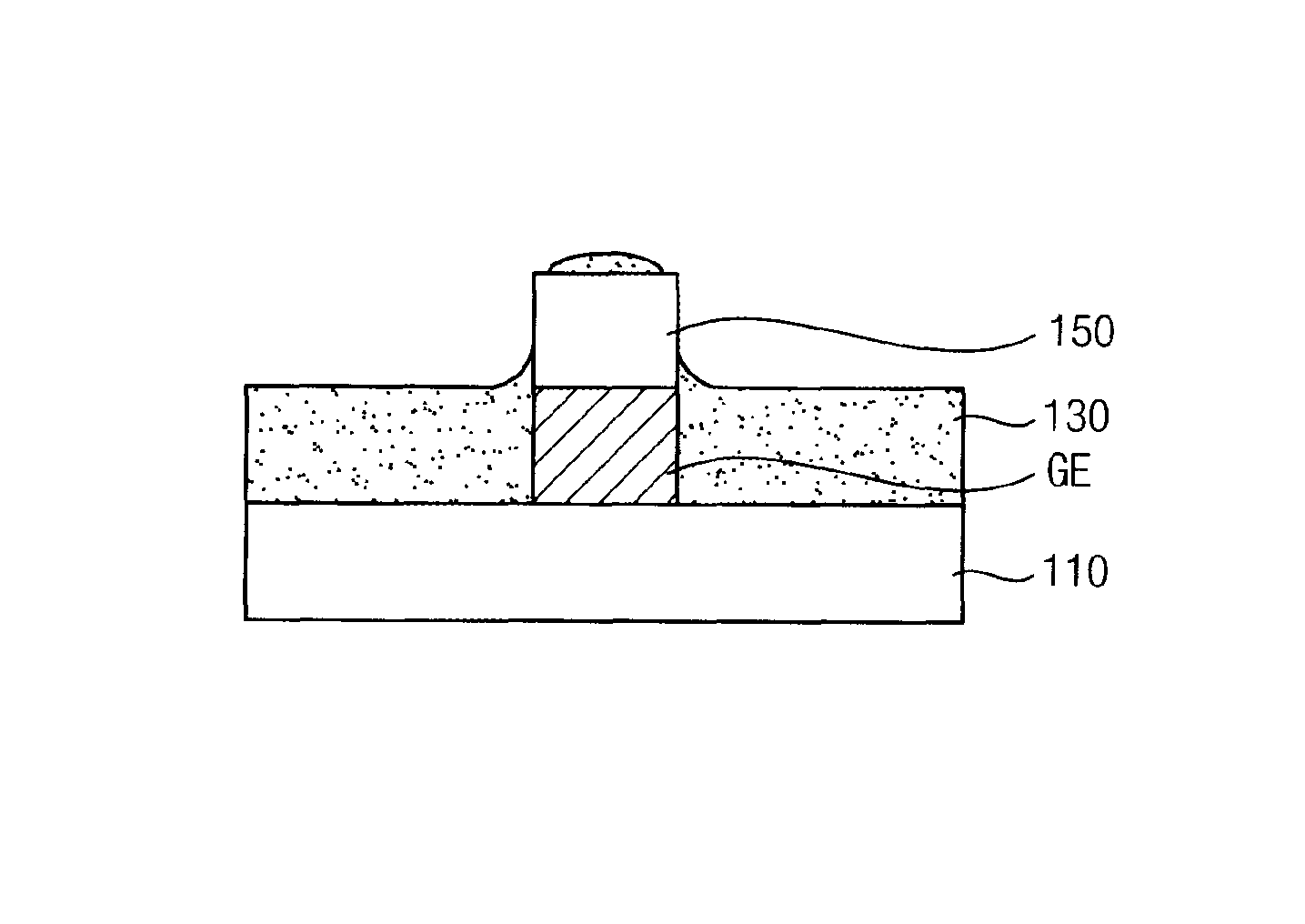
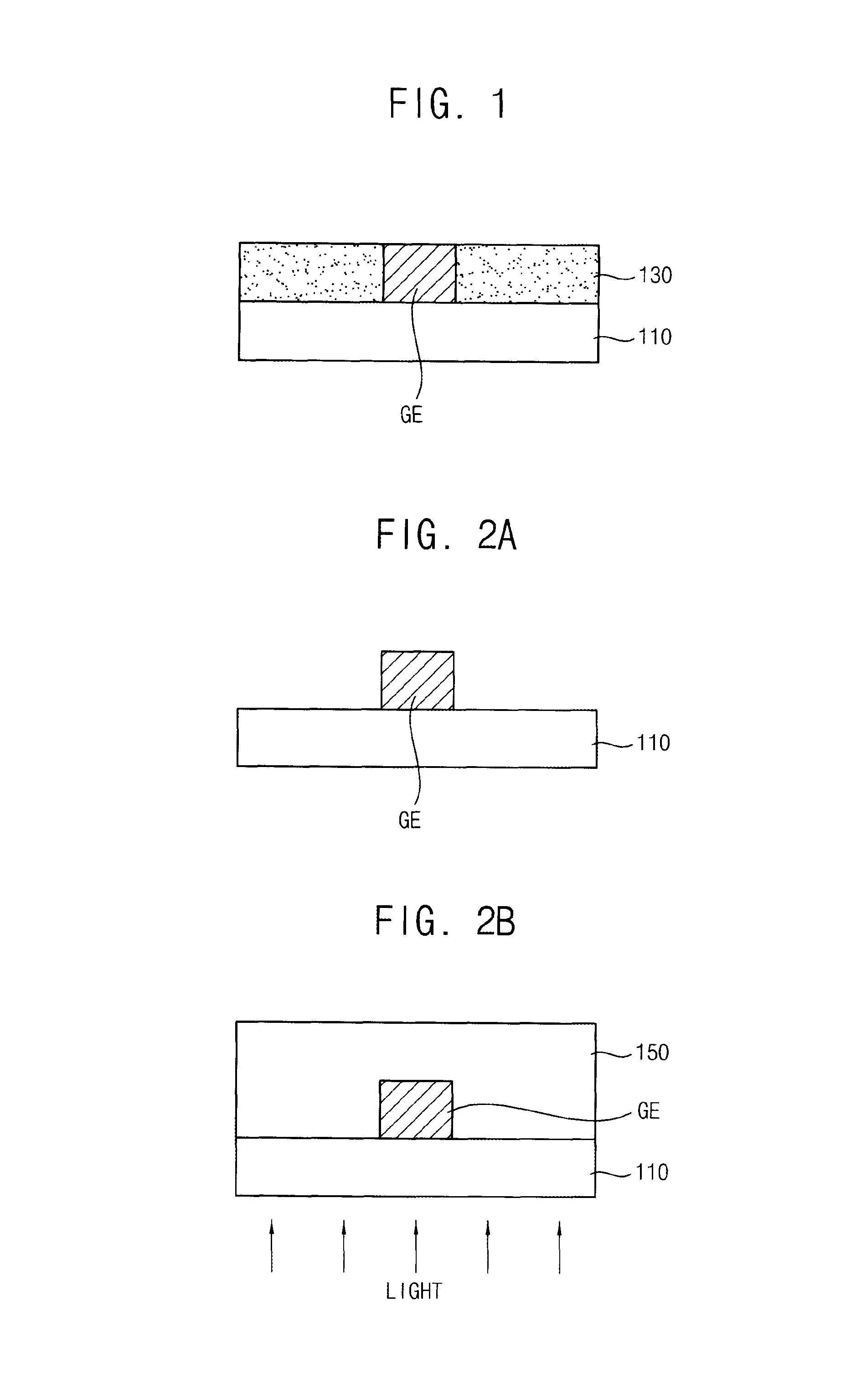
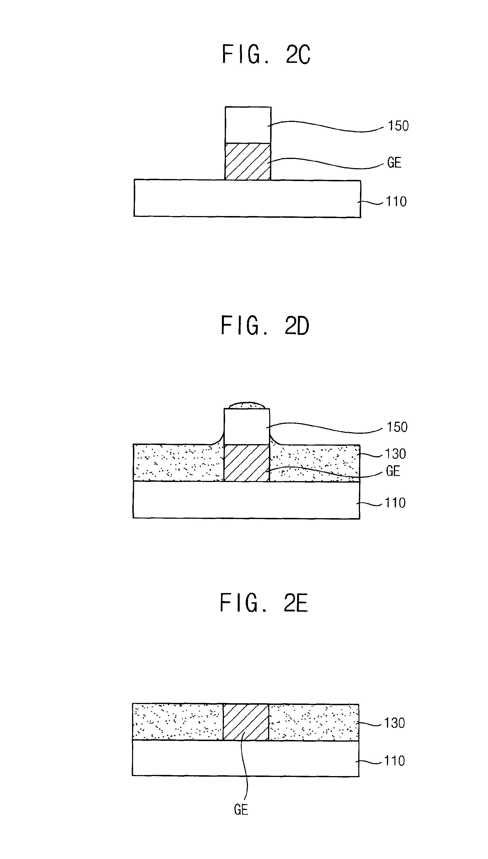
[0058]FIG. 1 is a cross-sectional view illustrating a substrate according to an exemplary embodiment.

[0059]Referring to FIG. 1, the substrate includes a base substrate 110, a conductive pattern GE and a planarizing layer 130 disposed on the base substrate 110. For example, the conductive pattern GE may be a gate electrode of a thin film transistor (“TFT”), which is a switching element of a display apparatus.

[0060]The conductive pattern GE may have a relatively thick thickness. For example, a thickness of the conductive pattern GE may be equal to or greater than about 1 μm. For example, a thickness of the conductive pattern GE may be between about 1 μm and about 3 μm.

[0061]The conductive pattern GE has a relatively thick thickness so that a resistance of the conductive pattern GE may decrease. Thus, a display panel may be driven in a relatively high speed. In addit...


PUM


Abstract

A method of planarizing a substrate includes forming a conductive pattern on a first surface of a base substrate, forming a positive photoresist layer on the base substrate and the conductive pattern, exposing the positive photoresist layer to light by irradiating a second surface of the base substrate opposite to the first surface with light, developing the positive photoresist layer to form a protruded portion on the conductive pattern, forming a planarizing layer on the base substrate and the protruded portion and eliminating the protruded portion.

Description

CROSS-REFERENCE TO RELATED APPLICATION[0001]This application claims priority to Korean Patent Application No. 10-2012-0014935, filed on Feb. 14, 2012, and all the benefits accruing therefrom under 35 U.S.C. §119, the contents of which in its entirety is herein incorporated by reference.BACKGROUND OF THE INVENTION[0002]1. Field of the Invention[0003]Exemplary embodiments relate to a method of planarizing a substrate and a method of manufacturing a thin film transistor using the method of planarizing a substrate. More particularly, exemplary embodiments relate to a method of planarizing a substrate to improve the reliability of a manufacturing process and a method of manufacturing a thin film transistor using the method of planarizing a substrate.[0004]2. Description of the Related Art[0005]Generally, a display apparatus includes an array substrate having a switching element and an opposite substrate facing the array substrate. The switching element includes a gate electrode electrica...

Claims


Application Information

Patent Timeline
Patent Type & Authority Patents(United States)
IPC IPC(8): H01L21/311H01L29/786H01L21/02H01L29/66H01L21/321H01L21/027
CPCH01L29/786H01L21/0274H01L21/02697H01L21/32115H01L29/66765H01L29/78603H01L29/7869H01L21/28123
Inventor KONG, HYANG-SHIKSHIM, SEUNG-BOJU, JIN-HOKIM, JUN-GI
Owner SAMSUNG DISPLAY CO LTD
Why Eureka
Try Eureka