

Method of planarizing substrate and method of manufacturing thin film transistor using the same
- Summary
- Abstract
- Description
- Claims
- Application Information
AI Technical Summary
Benefits of technology
Problems solved by technology
Method used
Image

Examples
Embodiment Construction
[0057]Hereinafter, exemplary embodiments will be described in further detail with reference to the accompanying drawings.
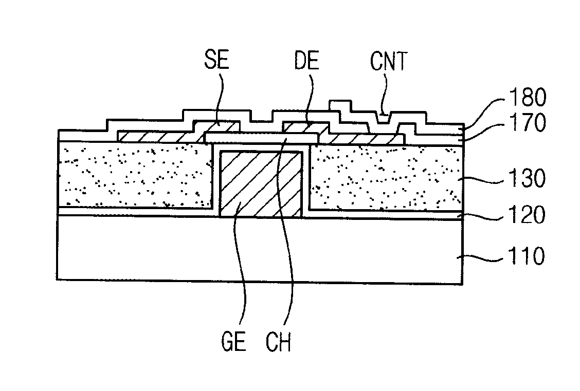
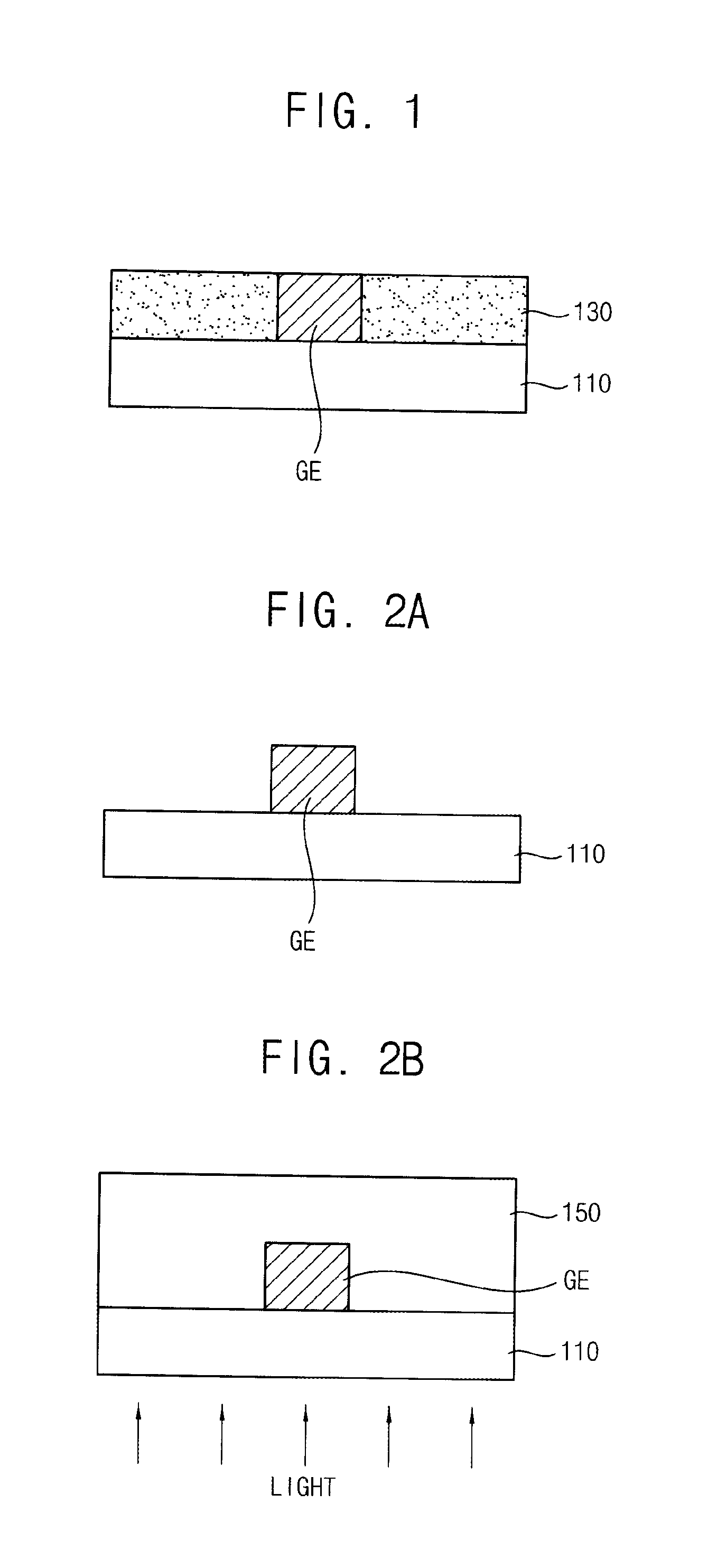
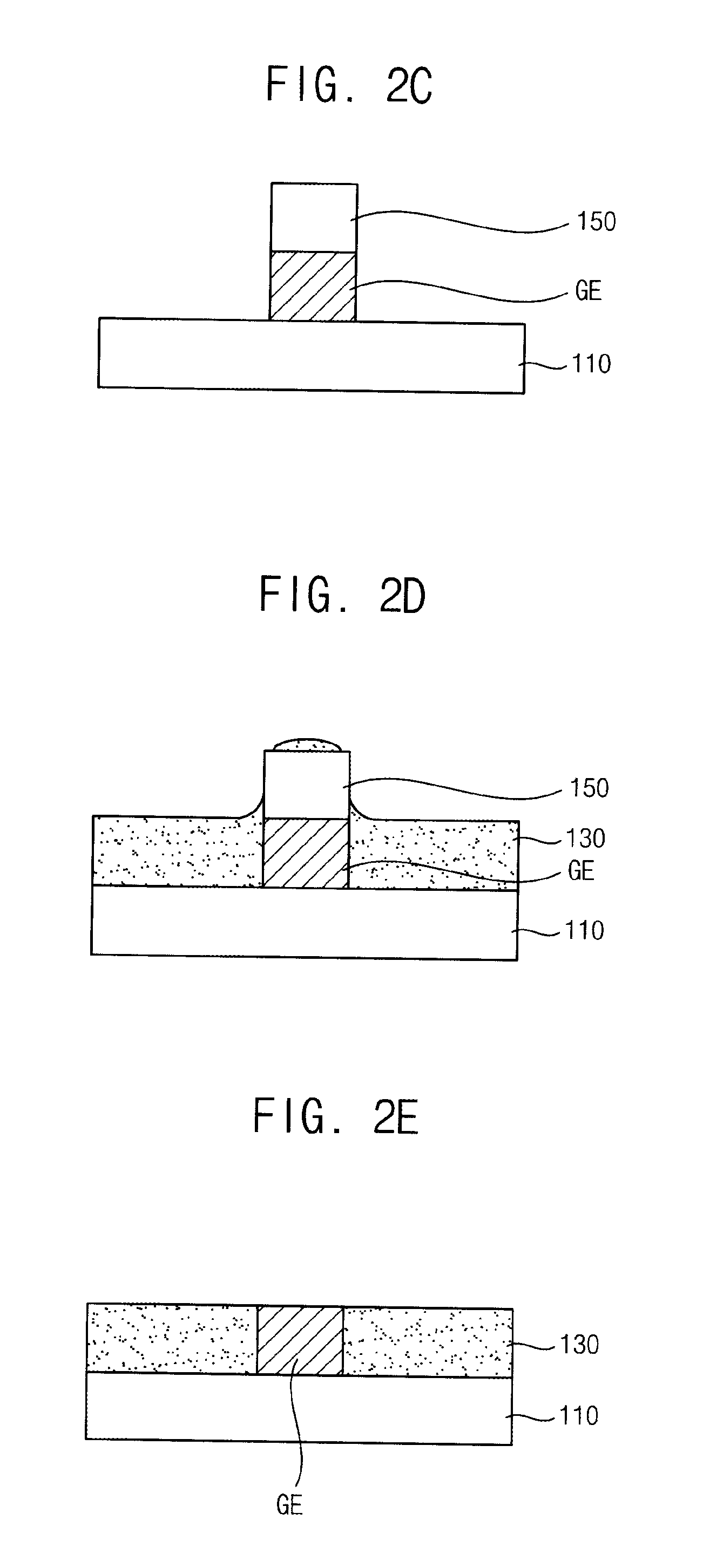
[0058]FIG. 1 is a cross-sectional view illustrating a substrate according to an exemplary embodiment.
[0059]Referring to FIG. 1, the substrate includes a base substrate 110, a conductive pattern GE and a planarizing layer 130 disposed on the base substrate 110. For example, the conductive pattern GE may be a gate electrode of a thin film transistor (“TFT”), which is a switching element of a display apparatus.
[0060]The conductive pattern GE may have a relatively thick thickness. For example, a thickness of the conductive pattern GE may be equal to or greater than about 1 μm. For example, a thickness of the conductive pattern GE may be between about 1 μm and about 3 μm.
[0061]The conductive pattern GE has a relatively thick thickness so that a resistance of the conductive pattern GE may decrease. Thus, a display panel may be driven in a relatively high speed. In addit...
PUM
 Abstract
Description
Claims
Application Information