Method for forming device isolation region

A technology for device isolation and peripheral circuit area, applied in semiconductor/solid-state device manufacturing, electrical components, circuits, etc., can solve the problems of insulating oxide layer depression, polysilicon residue, active device short circuit, etc., and achieve the effect of improving the depression situation.

Active Publication Date: 2009-12-30
SEMICON MFG INT (SHANGHAI) CORP +1
View PDF6 Cites 0 Cited by
  • Summary
  • Abstract
  • Description
  • Claims
  • Application Information

AI Technical Summary

Problems solved by technology

However, the peripheral circuit area is a non-dense area of ​​active devices, and the width of some shallow trenches is greater than 20um. After grinding the insulating oxide layer in shallow trenches of this width, serious depressions will occur, resulting in leakage currents, and further in subsequent processes. Generate polysilicon residues and cause short circuits between active devices

Method used


Image

  • Method for forming device isolation region
  • Method for forming device isolation region
  • Method for forming device isolation region

Examples


Embodiment Construction

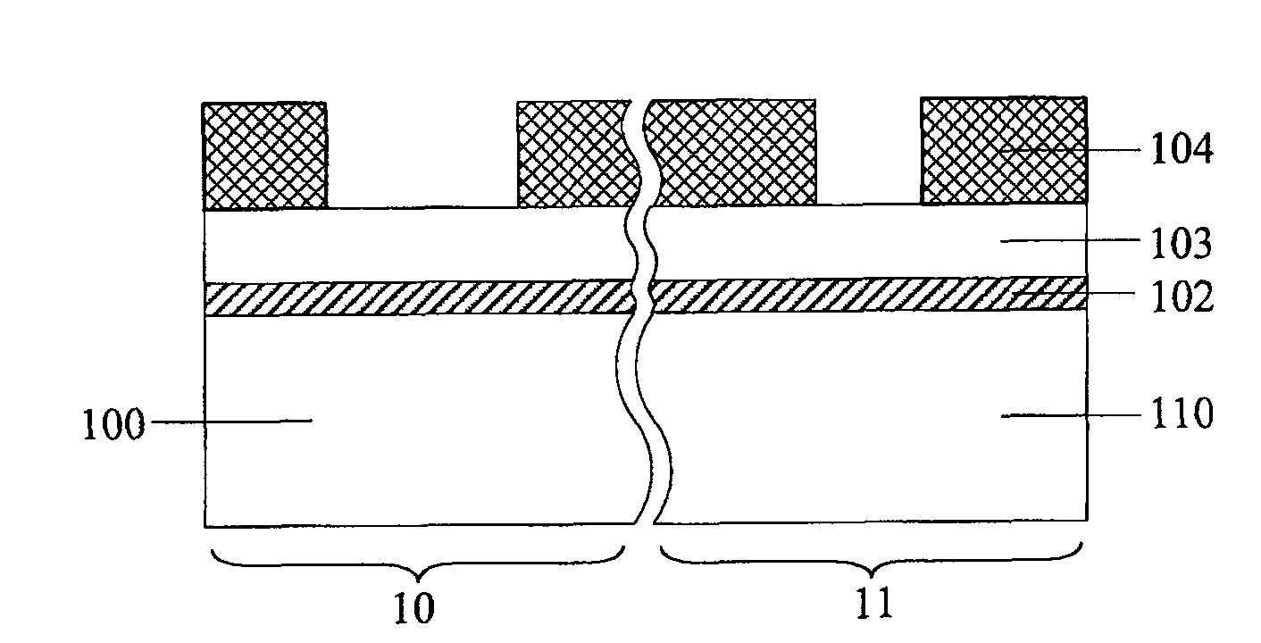
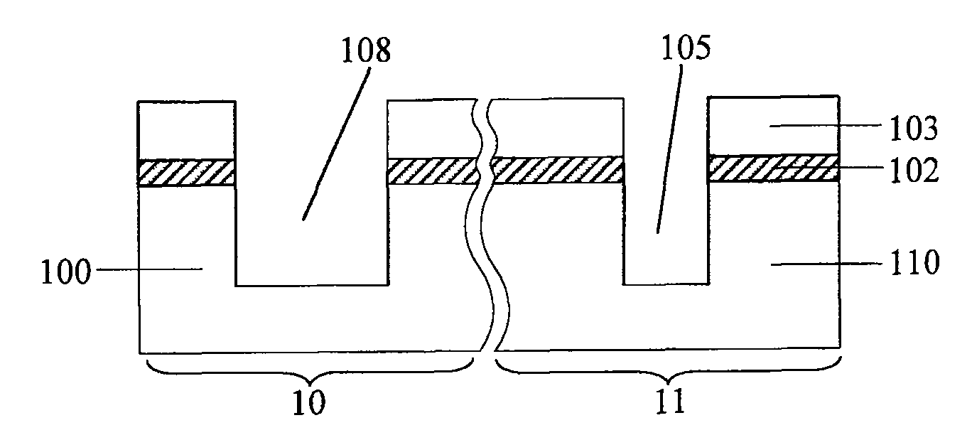
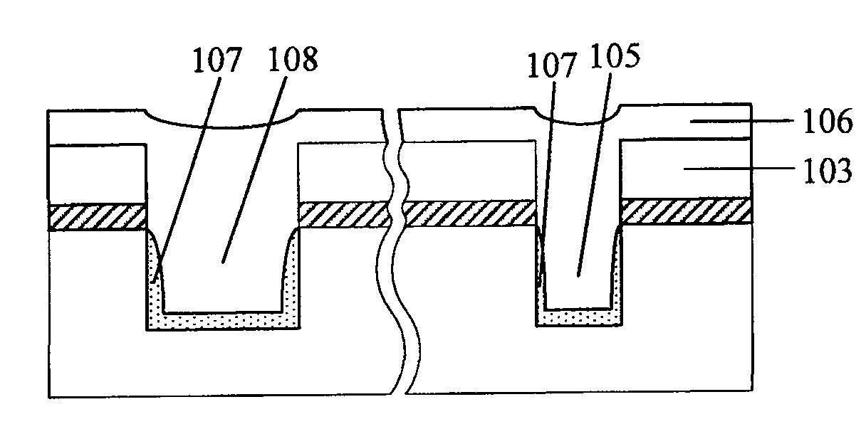
[0021] As the semiconductor technology enters the deep submicron era, the active area isolation of devices below 0.18 μm has mostly been produced by shallow trench isolation technology. Shallow trench isolation technology is an effective method to solve the "bird's beak" problem caused by local oxidation isolation in MOS circuits. However, due to the high aspect ratio of the shallow trenches of deep submicron components, and the high-density plasma chemical vapor deposition (HDP-CVD) method has two functions of "etching" and "deposition", so the process of deposition At the same time, an etching reaction to peel off the deposit will also be carried out, so that the high-density plasma chemical vapor deposition method has good trench filling ability, so it is applied to the insulating oxide layer in the formation of the shallow trench isolation structure.

[0022] Use high-density plasma chemical vapor deposition to fill the shallow trenches in the peripheral circuit area with ...


PUM

PropertyMeasurementUnit
thicknessaaaaaaaaaa
thicknessaaaaaaaaaa

Abstract

The invention relates to a method for forming a part isolating zone, firstly an oxidizing lining layer and a first silicon nitride layer are formed in turn on a silicon underlay, the oxidizing lining layer, the first silicon nitride and the silicon underlay are etched to form a groove, an insulating oxidizing layer is formed on the first silicon nitride layer, the insulating oxidizing layer can be filled fully in the groove; a second silicon nitride layer is formed on the insulating oxidizing layer, the second silicon nitride layer, the insulating oxidizing layer and the first silicon nitride layer are rubbed to remove the first silicon nitride layer and the oxidizing lining layer and form a shallow groove isolating structure. After the steps are finished, and because one silicon nitride layer is deposited on a silicon oxide layer, when the silicon oxide layer and the silicon nitride layer are rubbed, the speed for rubbing the silicon nitride is slower than that for rubbing the silicon oxide, thereby the depressed condition of the silicon oxide in the shallow groove can be improved after the rubbing process is over.

Description

technical field [0001] The invention relates to a method for forming device isolation regions, in particular to a manufacturing method for shallow trench isolation semiconductor devices. Background technique [0002] As the size of integrated circuits decreases, the devices that make up the circuits must be placed more densely to fit the limited space available on the chip. Since current research is devoted to increasing the density of active devices per unit area of ​​a semiconductor substrate, effective insulating isolation between circuits becomes more important. The methods for forming isolation regions in the prior art mainly include local oxidation isolation (LOCOS) process or shallow trench isolation (STI) process. The LOCOS process is to deposit a layer of silicon nitride on the surface of the wafer, and then perform etching to oxidize and grow silicon oxide in part of the recessed area, and the active device is generated in the area determined by the silicon nitrid...

Claims


Application Information

Patent Timeline
Patent Type & Authority Patents(China)
IPC IPC(8): H01L21/762
Inventor 蒋莉邹陆军李绍彬吴佳特
Owner SEMICON MFG INT (SHANGHAI) CORP
Why Eureka
Try Eureka