A method of fabricating a semiconductor structure

A manufacturing method and semiconductor technology, which is applied in semiconductor/solid-state device manufacturing, electrical components, circuits, etc., can solve problems such as slow deposition speed, decreased yield rate of semiconductor devices, and easy occurrence of dents, so as to improve dents and improve isolation effect, quality-enhancing effect

Active Publication Date: 2022-04-19
晶芯成(北京)科技有限公司 +1
View PDF0 Cites 0 Cited by
  • Summary
  • Abstract
  • Description
  • Claims
  • Application Information

AI Technical Summary

Problems solved by technology

In the conductor process, some devices include different functional areas, which have different requirements for the width of the shallow trench isolation structure. It is necessary to form shallow trench isolation structures with different widths in different regions of the chip, but shallow trenches with larger widths are deposited. The isolation dielectric is deposited at a slow rate, which causes depressions to occur during the formation of the shallow trench isolation structure, resulting in a decrease in the yield of semiconductor devices

Method used


Image

  • A method of fabricating a semiconductor structure
  • A method of fabricating a semiconductor structure
  • A method of fabricating a semiconductor structure

Examples


Embodiment Construction

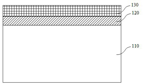
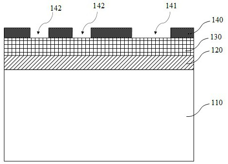
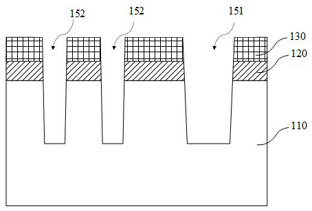
[0040] The following will clearly and completely describe the technical solutions in the embodiments of the present invention with reference to the accompanying drawings in the embodiments of the present invention. Obviously, the described embodiments are only some, not all, embodiments of the present invention. Based on the embodiments of the present invention, all other embodiments obtained by persons of ordinary skill in the art without creative efforts fall within the protection scope of the present invention.

[0041] It should be noted that the diagrams provided in this embodiment are only schematically illustrating the basic idea of ​​the present invention, and only the components related to the present invention are shown in the diagrams rather than the number, shape and shape of the components in actual implementation. Dimensional drawing, the type, quantity and proportion of each component can be changed arbitrarily during actual implementation, and the component layo...


PUM

PropertyMeasurementUnit
thicknessaaaaaaaaaa
thicknessaaaaaaaaaa
thicknessaaaaaaaaaa

Abstract

The invention discloses a method for manufacturing a semiconductor structure, comprising: providing a substrate; forming a first type shallow trench and a second type shallow trench on the substrate, and the first type shallow trench The opening area is larger than the opening area of ​​the second type shallow trench; a first lining layer is formed in the first type shallow trench and the second type shallow trench; in the second type shallow trench forming a second liner layer, and the second liner layer is disposed on the first liner layer; and depositing an isolation medium in the first type shallow trench and the second type shallow trench. The performance of the semiconductor structure can be improved through the manufacturing method of the semiconductor structure provided by the invention.

Description

technical field [0001] The invention belongs to the technical field of semiconductors, in particular to a method for manufacturing a semiconductor structure. Background technique [0002] A shallow trench isolation structure (Shallow Trench Isolation, STI) is an important structure in an integrated circuit, which can prevent current leakage between adjacent semiconductor devices and play a role in other electrical properties. In the conductor process, some devices include different functional areas, which have different requirements for the width of the shallow trench isolation structure. It is necessary to form shallow trench isolation structures with different widths in different regions of the chip, but shallow trenches with larger widths are deposited. The deposition rate of the isolation dielectric is relatively slow, which causes depressions to occur easily during the formation of the shallow trench isolation structure, resulting in a decrease in the yield of the semic...

Claims


Application Information

Patent Timeline
Patent Type & Authority Patents(China)
IPC IPC(8): H01L21/762
CPCH01L21/76224H01L21/76229
Inventor 朱瑶
Owner 晶芯成(北京)科技有限公司
Why Eureka
Try Eureka