Method for manufacturing shell of electronic product

A manufacturing method and technology of electronic products, applied in the direction of electrical equipment shell/cabinet/drawer, electrical components, etc., can solve the problems of inability to effectively guarantee the electroplating process, difficult laser activation process, exposure of metal particles, etc., to reduce poor appearance, enhance Competitiveness, the effect of reducing manufacturing costs

Active Publication Date: 2014-04-02
KUNSHAN RUIXIANG XUNTONG COMM TECHCO
View PDF4 Cites 24 Cited by
  • Summary
  • Abstract
  • Description
  • Claims
  • Application Information

AI Technical Summary

Problems solved by technology

[0007] However, the process proposed in the Chinese patent application also has problems: since LDS uses a laser to carve the circuit traces of the antenna on the surface of the thermoplastic composite component, the organic metal additive in the thermoplastic material is activated by the laser, and the organic The metal particles in the metal additive are exposed on the surface of the circuit trace of the component, and finally the laser-activated part of the component is metal-coated, thereby forming a mobile phone antenna of a specific shape on the surface of the component
In the conventional LDS process, usually after laser activation, the depth of the shallow groove formed on the surface of the electronic device casing can only ensure the realization of the subsequent electroplating process, usually only 1-2μm, and the Chinese patent application is to make the shallow groove Changed to a deep groove of 16-20μm, the depth is an order of magnitude higher than the original one, which is a very difficult task for the laser activation process
Although the patent application claims that when a specific type of equipment is used to select a laser with a specific wavelength, a specific marking speed, a specific Q frequency, a specific rated power of the device, a specific current and a specific line spacing, it can be better formed. described grooves, but the formation of the grooves still seems to be time-consuming and laborious
Moreover, during the process of laser activation, metal particles will be exposed, and further deepening the groove with laser will inevitably cause the activated metal to be oxidized, thereby losing its conductivity, resulting in the inability to effectively guarantee the subsequent electroplating process.

Method used


Image

  • Method for manufacturing shell of electronic product
  • Method for manufacturing shell of electronic product
  • Method for manufacturing shell of electronic product

Examples


Embodiment Construction

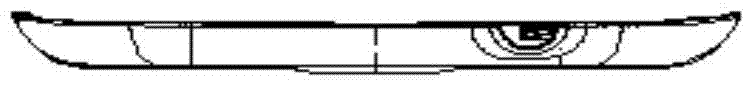
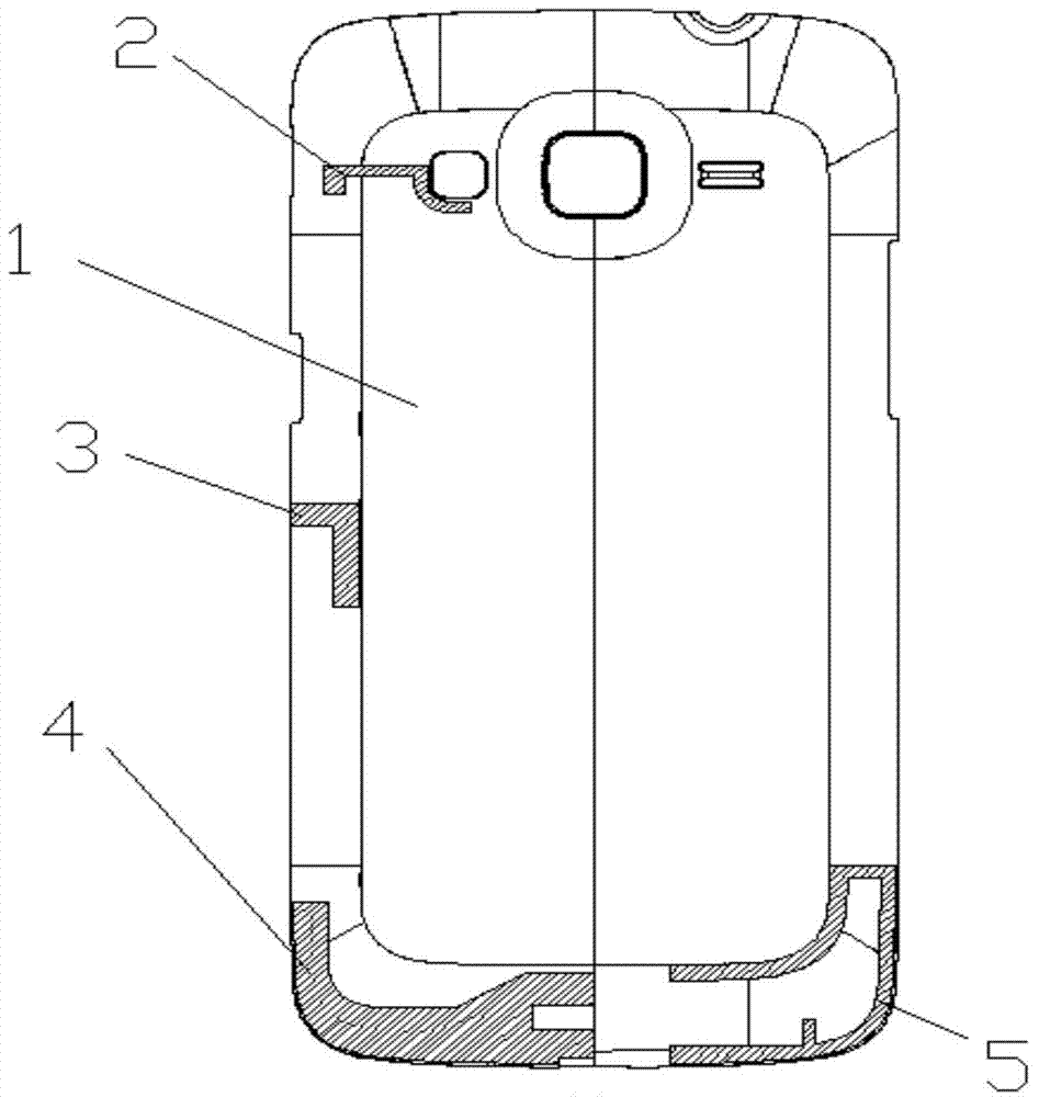
[0016] The manufacturing method of the electronic product shell of the present embodiment is: provide one or more sets of mobile phone antennas that need to be assembled or printed on the plastic molding mold on the surface, reserve a groove of corresponding depth at the antenna forming position, and process the antenna that needs to be assembled or printed. On the surface of the plastic product or in the groove of the inner wall, the surface is currently sprayed; the spraying process is: primer + intermediate paint 1 + intermediate paint 2 + intermediate paint 3 + top coat. Cancel the production process that requires sandblasting during the spraying process.

[0017] Its specific process steps include:

[0018] 1. The injection mold is designed in 3D drawing: the design plan is: firstly, the installation position of the antenna should be designed according to the function of the antenna. The design of the antenna should be far away from the main part of the battery, and the p...


PUM

PropertyMeasurementUnit
depthaaaaaaaaaa
depthaaaaaaaaaa
depthaaaaaaaaaa

Abstract

The invention discloses a method for manufacturing a shell of an electronic product. The method comprises the following steps of A, generating of 3D (Three-Dimensional) drawing file design of an injection mold: reserving an antenna groove by the injection mold when a mold opening 3D drawing file design is generated; B, injection mold processing: carrying out shape processing on the antenna groove when a mold core is processed so as to ensure the integrated forming of an antenna and the shell of the product when the antenna is subsequently processed, and enabling the shell of the product not to be subjected to poor appearance when surface processing is carried out; C, injection molding machine molding: completing the injection molding of the product by utilizing the injection mold, which is already designed and processed in a mold, of the antenna groove; D, mobile phone antenna processing: directly processing a mobile phone antenna in the antenna groove on the surface or the inner wall of a mobile phone plastic piece; E, mobile phone surface processing and coating. According to the method disclosed by the invention, the bottlenecks of a surface decoration technology that the surface of the product is rugged when the mobile phone antenna is assembled or printed on the surface of the product, and the surface of the product needs to be sanded when the mobile phone antenna is produced can be broken through, highly-textured appearance on the surface of the product can be generated, the manufacturing cost can be reduced, and the yield of the product can be increased.

Description

technical field [0001] The invention relates to a method for manufacturing an electronic product casing, in particular to a method for manufacturing an electronic product casing with an antenna. Background technique [0002] With the progress of society, everyone has a new requirement for various consumer goods, especially 3C electronic products, and the consumption of 3C products has become an indispensable part of people's material life. Products with high-gloss, high-brightness, diversified metal shells and surface metal plating appearances that appear in the consumer market are favored by consumers. This is the case with mobile phones, for example. [0003] The evolution of mobile phones is no longer just a simple communication tool. After years of technological evolution, it has evolved from a single communication function to a highly intelligent terminal that integrates functions such as Internet access, navigation, real-time video, wireless transmission, and communic...

Claims


Application Information

Patent Timeline
Patent Type & Authority Applications(China)
IPC IPC(8): H05K5/00B29C45/00
Inventor 周洪波彭万春康银超黎声田
Owner KUNSHAN RUIXIANG XUNTONG COMM TECHCO
Why Eureka
Try Eureka