Mask set, thin film transistor, manufacturing method of thin film transistor, array substrate and display device

A thin-film transistor and mask technology, which is applied in the manufacture of transistors, semiconductor/solid-state devices, and electric solid-state devices, etc., can solve the problems of small display screen brightness, large coverage area, and low light transmittance of display devices. The effect of increasing the size value

Active Publication Date: 2014-04-09
BEIJING BOE OPTOELECTRONCIS TECH CO LTD
View PDF3 Cites 8 Cited by
  • Summary
  • Abstract
  • Description
  • Claims
  • Application Information

AI Technical Summary

Problems solved by technology

[0007] Embodiments of the present invention provide a mask plate set, a thin film transistor and its manufacturing method, an array substrate, and a display device to solve the problem in the prior art that the coverage area of ​​the black matrix in each pixel unit is relatively large, so that The transmittance of light is relatively small, so that the brightness of the display screen of the display device is relatively small

Method used


Image

  • Mask set, thin film transistor, manufacturing method of thin film transistor, array substrate and display device
  • Mask set, thin film transistor, manufacturing method of thin film transistor, array substrate and display device
  • Mask set, thin film transistor, manufacturing method of thin film transistor, array substrate and display device

Examples


Embodiment 1

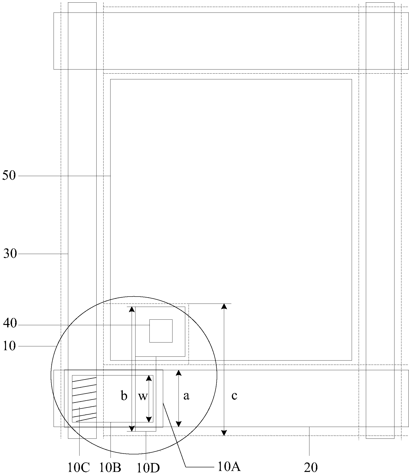
[0076] In Embodiment 1 of the present invention, the shape of the active layer is a regular shape, such as an isosceles trapezoid.

[0077] Preferably, the active layer is an isosceles trapezoid, the base of the isosceles trapezoid is located in a direction parallel to the data line, and the upper base of the isosceles trapezoid is located between the drain electrode and the active layer. The overlapping area of ​​the layer, the lower base of the isosceles trapezoid is located in the overlapping area of ​​the source electrode and the active layer; wherein the size value of the upper base and the lower base of the isosceles trapezoid conforms to the thin film transistor performance requirements.

[0078] In a specific implementation, since the active layer of the TFT is the isosceles trapezoid, the overlapping area between the drain electrode and the active layer is an isosceles trapezoid whose bottom is in a direction parallel to the data line, and The upper base of the overl...

Embodiment 2

[0110] In Embodiment 2 of the present invention, the shape of the active layer is a regular shape, for example, the shape is a simple deformation of an isosceles trapezoid, that is, a shape similar to an isosceles trapezoid.

[0111] Preferably, the shape of the active layer is similar to an isosceles trapezoid, at least one side of which is a curve.

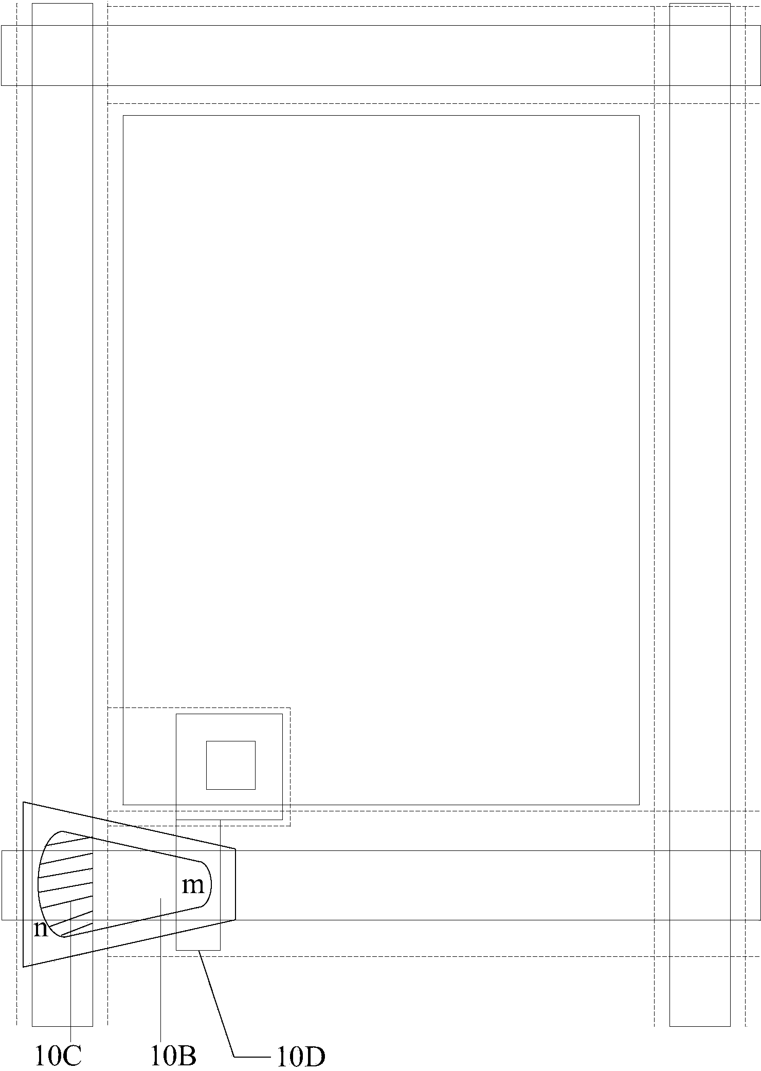
[0112] For example, if Figure 2B As shown, one side (ie, side m) of the active layer 10B located in the overlapping area of ​​the active layer 10B and the drain electrode 10D, and one side (ie, side m) located in the overlapping area of ​​the active layer 10B and the source electrode 10C n) is a curve;

[0113] like Figure 2C As shown, two sides (ie, sides x and y) of the active layer 10B overlapping the data line 30 and the drain electrode 10D at the same time are curved lines.

[0114] It should be noted that, when the shape of the active layer is similar to an isosceles trapezoid, at least one side thereof can be not onl...

Embodiment 3

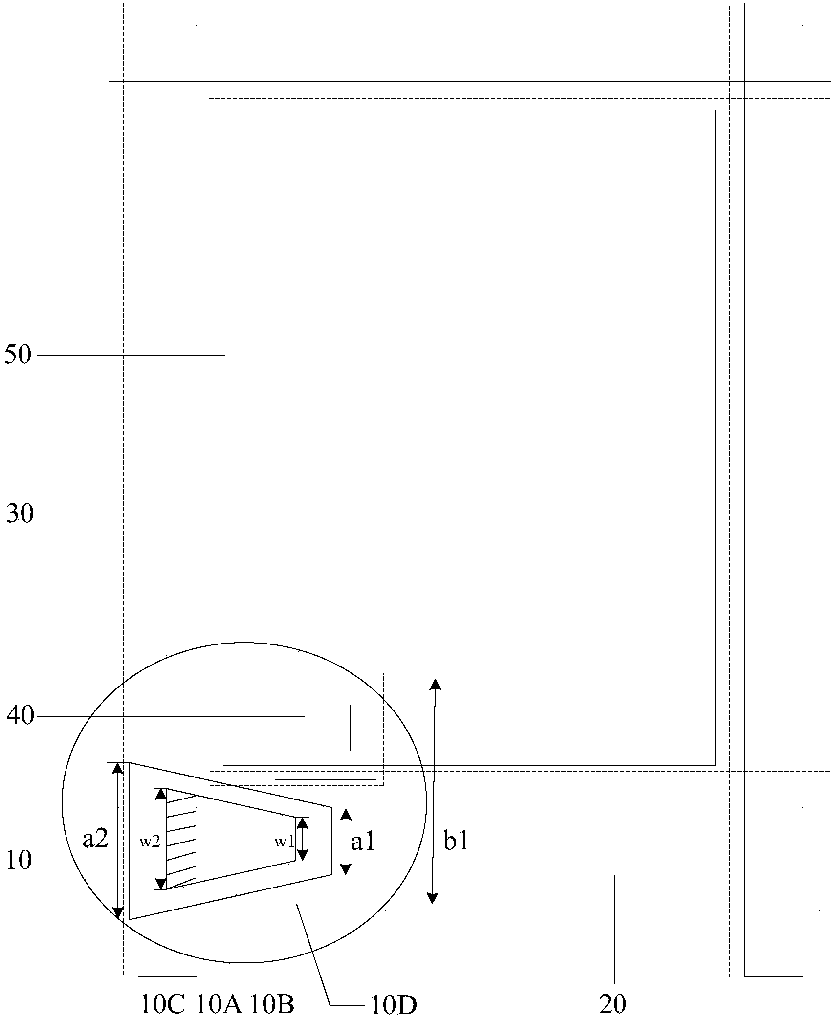
[0117] In Embodiment 3 of the present invention, the shape of the active layer is a regular shape, for example, other trapezoids than the isosceles trapezoid.

[0118] For example, if Figure 2D As shown, the active layer 10B is a right-angled trapezoid, the bottom of the active layer 10B is located in a direction parallel to the data line 30, and the upper bottom of the active layer 10B is located in the overlapping area of ​​the drain electrode 10D and the active layer 10B. The lower bottom edge of the active layer 10B is located in the overlapping region of the source electrode 10C and the active layer 10B; wherein, the size value of the upper bottom edge of the active layer 10B is z1, and the size value of the lower bottom edge of the active layer 10B is z1. z2, z1 and z2 meet the performance requirements of TFT10.

[0119] It should be noted that, similar to Embodiment 2 of the present invention, the shape of the active layer may be a shape similar to a right-angled trap...


PUM


Abstract

The invention relates to the technical field of displaying, in particular to a mask set, a thin film transistor, a manufacturing method of the thin film transistor, an array substrate and a display device in order to solve the problem that a display screen of a display device is low in luminance. According to the thin film transistor, the maximum size value of an overlapping area of an active layer and a drain electrode of the thin film transistor in the direction parallel with a data line is smaller than the size value of one side overlapped with the data line in an overlapping area of the active layer and a source electrode, wherein the source electrode is a data line part located in the overlapping area of the active layer and the data line. According to the embodiment, an opening area of a pixel unit is enlarged, the light transmittance is improved, and the luminance of a display screen of the display device comprising the pixel units becomes higher. The problem that the picture flickers is avoided to a certain extent, and the picture display quality is improved.

Description

technical field [0001] The invention relates to the field of display technology, in particular to a mask plate set, a thin film transistor and a manufacturing method thereof, an array substrate, and a display device. Background technique [0002] The current array substrate of a display device generally includes a base substrate, a plurality of parallel gate lines located inside the base substrate, and a plurality of data lines vertically intersecting and electrically insulated from the gate lines, wherein two adjacent gate lines A line and two adjacent data lines form a pixel unit. Each pixel unit surrounded by two adjacent gate lines and two adjacent data lines includes a TFT (Thin Film Transistor, thin film transistor) for driving image display and a pixel electrode connected to the TFT. [0003] Taking the TFT of the pixel unit as a TFT with a bottom gate structure as an example, such as figure 1 As shown, the TFT 10 of the pixel unit includes a gate electrode 10A loca...

Claims


Application Information

Patent Timeline
Patent Type & Authority Applications(China)
IPC IPC(8): H01L21/336H01L21/28H01L29/786H01L29/06H01L29/417G03F1/00
CPCG03F1/60H01L27/1214H01L29/0684H01L29/66742H01L29/786G02F1/136286G02F2201/40H01L27/1222H01L27/124H01L27/1288H01L29/41733H01L29/42384H01L29/78696G03F1/38
Inventor 薛艳娜董学陈小川薛海林
Owner BEIJING BOE OPTOELECTRONCIS TECH CO LTD
Why Eureka
Try Eureka