Complementary Metal-Oxide-Semiconductor Anti-Latch-Up Structure

An oxide semiconductor, complementary technology, used in semiconductor devices, transistors, electrical solid devices, etc., can solve the problems of limited protection capability, limited effective area of ​​the protective layer, single latch protection structure, etc., to increase the effective area, The effect of improving the discharge current capability and improving the latch protection capability

Active Publication Date: 2016-08-17
SHANGHAI HUAHONG GRACE SEMICON MFG CORP
View PDF3 Cites 0 Cited by
  • Summary
  • Abstract
  • Description
  • Claims
  • Application Information

AI Technical Summary

Problems solved by technology

Its protection mainly uses one side, which can play a certain effect on the protection of the latch, but this kind of latch protection structure is single, the effective area of ​​the protection layer is limited, and its protection ability is limited

Method used


Image

  • Complementary Metal-Oxide-Semiconductor Anti-Latch-Up Structure
  • Complementary Metal-Oxide-Semiconductor Anti-Latch-Up Structure
  • Complementary Metal-Oxide-Semiconductor Anti-Latch-Up Structure

Examples


Embodiment Construction

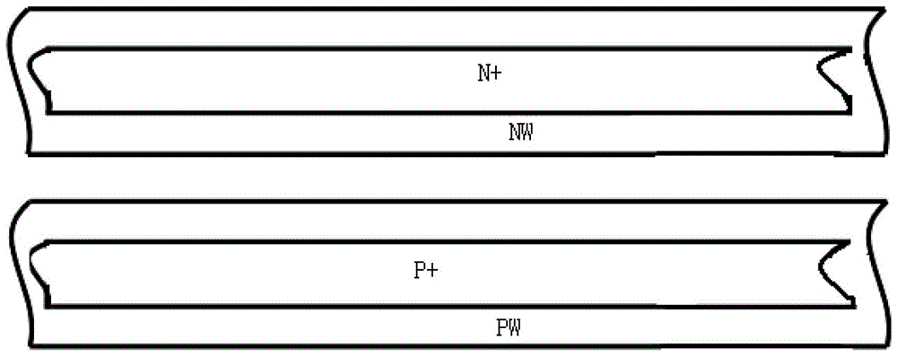
[0031] The complementary metal oxide semiconductor anti-latch-up structure of the present invention includes: an N-type latch-up protection layer and a P-type latch-up protection layer; wherein: the N-type latch-up protection layer can be composed of an N-type deep well and an N-type buried layer of the device , N well, and N-type diffusion region; the P-type latch protection layer can be composed of one or more of the P-type deep well, P-type buried layer, P well, and P-type diffusion region of the device;

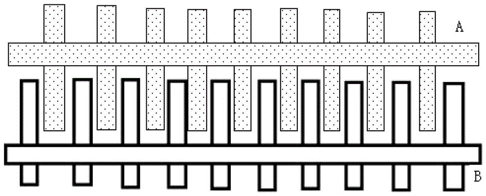
[0032] Such as figure 2 As shown, wherein, the N-type latch protection layer and the P-type latch protection layer are arranged in multiple groups in a cross shape.

[0033] The width of the N-type latch protection layer and the P row latch protection layer is between 0.5 um and 50 um, preferably 10 um, 20 um, 25.25 um, 30 um, and 40 um.

[0034] The length of the intersection of the N-type latch protection layer and the P-type latch protection layer is between 0.5um an...


PUM


Abstract

The invention discloses a complementary metal oxide semiconductor anti-latch structure which is composed of an N-type latch protection layers and a P-type latch protection layer. The N-type latch protection layer is composed of one or more of an N-type deep well, an N-type buried layer, an N well and an N-type diffusion region. The P-type latch protection layer is composed of one or more of a P-type deep well, a P-type buried layer, a P well and a P-type diffusion region. The N-type latch protection layer and the P-type latch protection layer are arranged into multiple groups and are cross-shaped. Compared with the exiting complementary metal oxide semiconductor anti-latch structure, the electrostatic protection turn-on voltage can be reduced, and the current discharge capability can be improved.

Description

technical field [0001] The invention relates to the field of semiconductor manufacturing, in particular to a complementary metal oxide semiconductor anti-latch structure. Background technique [0002] On a chip of a complementary metal-oxide-semiconductor process, there are usually several P-type and N-type transistors (PMOS and NMOS) at the same time. Therefore, there must be several parasitic P-N-P-N structure (P+ / NW / Psub / N+) Silicon-controlled rectifier (SCR) devices between the power line and the ground line. The latch has two current modes, one is to inject positive current on the I / O (input / output) pin, and the other is to inject negative current on the I / O pin. Such as image 3 As shown, taking the latch triggered by positive current injection as an example, the silicon controlled rectifier is composed of the following structure, (1) P+ diffusion region connected to VDD in the N well; (2) N well region; (3) P-type lining Bottom or P well region; (4) P-type substrate...

Claims


Application Information

Patent Timeline
Patent Type & Authority Patents(China)
IPC IPC(8): H01L27/092H01L27/02
Inventor 苏庆王邦麟苗彬彬邓樟鹏
Owner SHANGHAI HUAHONG GRACE SEMICON MFG CORP
Why Eureka
Try Eureka