Grid mould for emission imaging device, detector and emission imaging device

A technology for imaging equipment and detectors, applied in radiation measurement, X/γ/cosmic radiation measurement, instruments, etc., can solve the problems of difficult to achieve cutting technology, and achieve the effect of improving the performance of the detector

Active Publication Date: 2014-06-25
ZHONGPAI S&T SHENZHEN CO LTD
View PDF4 Cites 14 Cited by
  • Summary
  • Abstract
  • Description
  • Claims
  • Application Information

AI Technical Summary

Problems solved by technology

As for the depth of the groove 121, as mentioned above, in order to obtain the best crystal decoding effect, there is a certain accuracy requirement for the depth of the groove 121 (such as 200 micron precision), which is difficult to meet with traditional cutting techniques.

Method used


Image

  • Grid mould for emission imaging device, detector and emission imaging device
  • Grid mould for emission imaging device, detector and emission imaging device
  • Grid mould for emission imaging device, detector and emission imaging device

Examples


Embodiment Construction

[0035] In the following description, numerous specific details are given in order to provide a more thorough understanding of the present invention. It will be apparent, however, to one skilled in the art that the present invention may be practiced without one or more of these details. In other examples, some technical features known in the art are not described in order to avoid confusion with the present invention.

[0036] In order to provide a thorough understanding of the present invention, the detailed structure will be set forth in the following description. Obviously, the embodiments of the invention are not limited to specific details familiar to those skilled in the art. Preferred embodiments of the present invention are described in detail below, however, the present invention may have other embodiments besides these detailed descriptions.

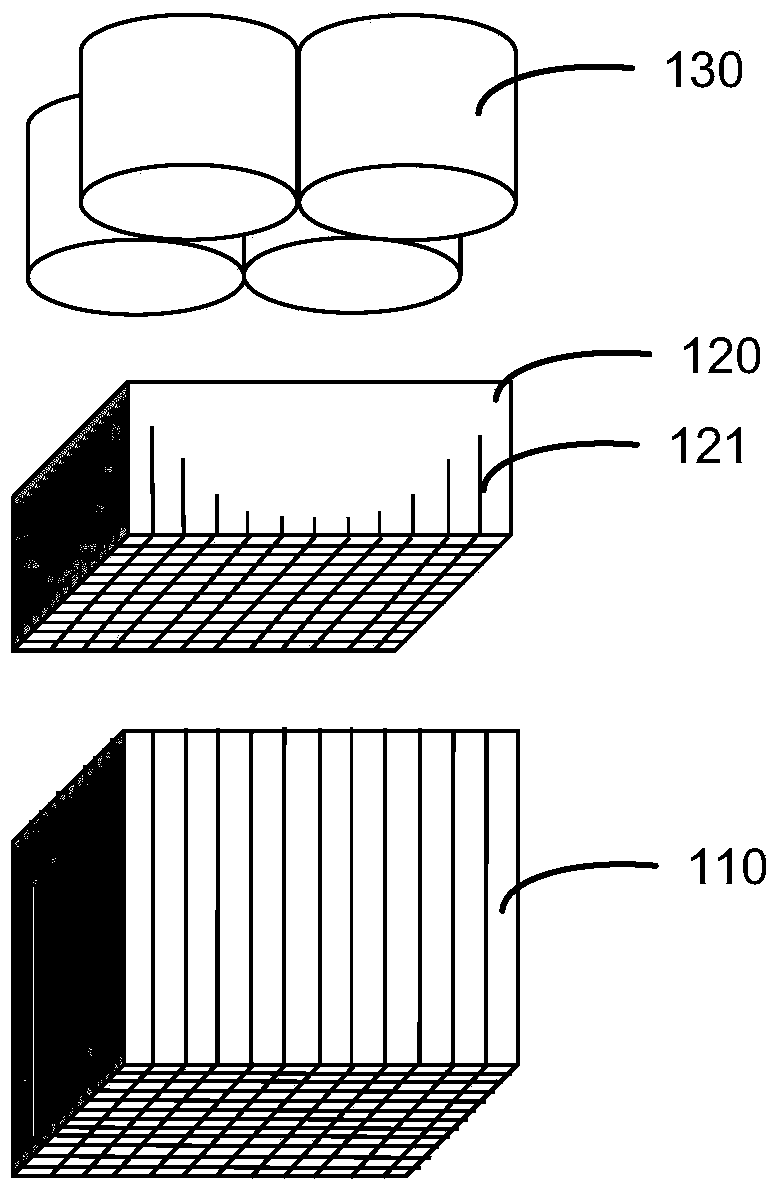
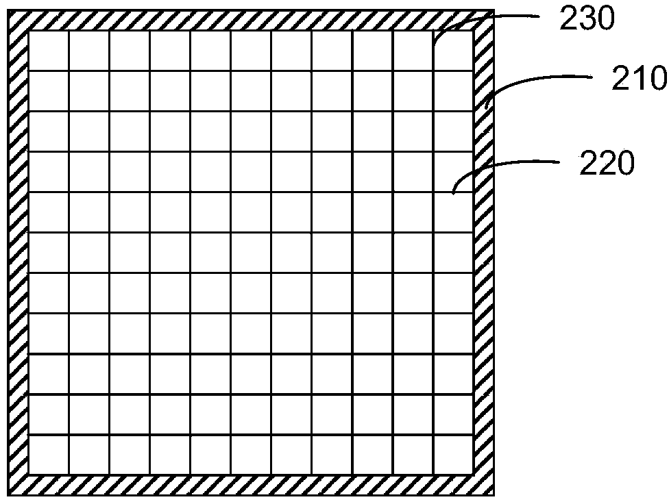
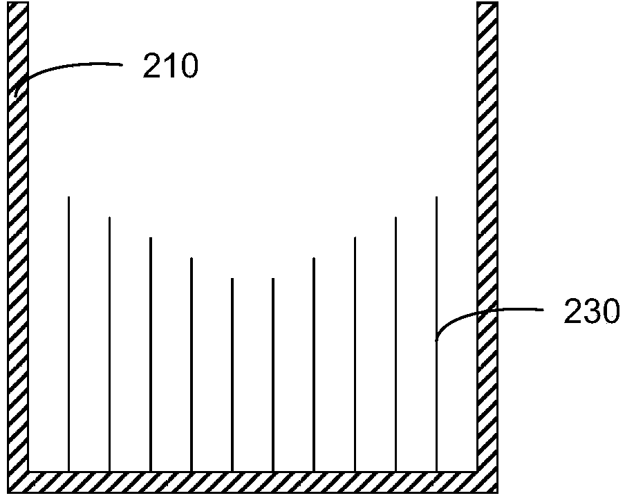
[0037] The present invention provides a grid mold for a detector of an emission imaging device, the grid mold is mainly used...


PUM


Abstract

The invention provides a grid mould for an emission imaging device, a detector and an emission imaging device. The grid mould comprises a shell, multiple transverse walls and multiple longitudinal walls, wherein the transverse walls are located in the shell and transversely extend along the shell in parallel, the longitudinal walls are located in the shell and longitudinal extend along the shell in parallel, the transverse walls and the longitudinal walls divide a lower space in the shell into multiple grid grooves distributed in a matrix mode, and the heights of the transverse walls and the longitudinal walls are gradually reduced from the periphery of the shell to the center of the shell. The heights of the transverse walls and the longitudinal walls are precisely measured, the grid mould can accurately control projection distribution of visible photon groups generated due to high-energy photon annihilation, and accordingly the best crystal decoding effect can be achieved. The grid mould can be manufactured by assembling the transverse walls and the longitudinal walls such as sheets, precise control over surface performance, appearance and the size can be achieved, and performance of the detector is remarkably improved.

Description

technical field [0001] The present invention relates to an emission imaging system, in particular to a grid mold for a detector of an emission imaging device, a detector with the grid mold, and an emission imaging device with the detector. Background technique [0002] Emission imaging devices, including positron emission imaging devices, have been used for medical diagnosis. Taking positron emission imaging equipment as an example, it uses the phenomenon that the positrons produced by the decay of positron isotopes and the negative electrons in the human body have an annihilation effect, leading to the injection of compounds labeled with positron isotopes into the human body, using the method of composite detection , using a detector to detect the annihilation effect produced by γ The photons can obtain the distribution information of isotopes in the human body, and the computer can reconstruct and combine operations to obtain a three-dimensional tomographic image of the d...

Claims


Application Information

Patent Timeline
Patent Type & Authority Applications(China)
IPC IPC(8): G01T1/29G01T1/202A61B6/03
CPCG01T1/202
Inventor 许剑锋石涵黄秋
Owner ZHONGPAI S&T SHENZHEN CO LTD
Why Eureka
Try Eureka